Rainbow Electronics MAX861 User Manual
Page 2
MAX860/MAX861
50mA, Frequency-Selectable,
Switched-Capacitor Voltage Converters
2
_______________________________________________________________________________________
ABSOLUTE MAXIMUM RATINGS
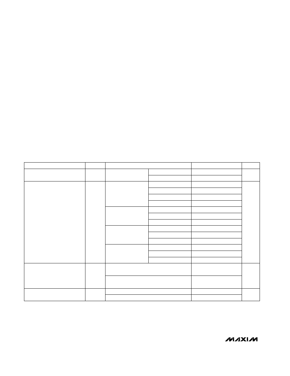
ELECTRICAL CHARACTERISTICS
(Typical Operating Circuit (Inverter), V
DD
= +5V,
–
S
—
H
—
D
—
N
–
= V
DD
, FC = LV = GND, C1 = C2 = 10µF (Note 2), T
A
= T
MIN
to T
MAX
, unless
otherwise noted. Typical values are at T
A
= +25°C.)
Stresses beyond those listed under “Absolute Maximum Ratings” may cause permanent damage to the device. These are stress ratings only, and functional
operation of the device at these or any other conditions beyond those indicated in the operational sections of the specifications is not implied. Exposure to
absolute maximum rating conditions for extended periods may affect device reliability.
Supply Voltage (V
DD
to GND or GND to OUT) ...................+6.0V
Input Voltage Range (LV, FC,
–
S
—
H
—
D
—
N
–
) ...................(OUT - 0.3V)
to (V
DD
+ 0.3V)
Continuous Output Current (OUT, V
DD
) .............................60mA
Output Short-Circuit to GND (Note 1)...................................1sec
Continuous Power Dissipation (T
A
= +70°C)
SO (derate 5.88mW/°C above +70°C) .........................471mW
µMAX (derate 4.10mW/°C above +70°C) ....................330mW
CERDIP (derate 8.00mW/°C above +70°C) .................640mW
Operating Temperature Ranges
MAX86_I_A ......................................................-25°C to +85°C
MAX86_ESA.....................................................-40°C to +85°C
MAX86_MJA ..................................................-55°C to +125°C
Storage Temperature Range .............................-65°C to +160°C
Lead Temperature (soldering, 10sec) .............................+300°C
I
L
= 10mA, V
DD
= 2V
R
L
= 1k
Ω
I
L
= 50mA
V
DD
= 3V, V
OUT
more negative than -2.5V
V
DD
= 5V, V
OUT
more negative than -3.75V
MAX861M
MAX860M
MAX861I/E
MAX860I/E
CONDITIONS
Ω
20
35
R
OUT
Output Resistance
(Note 3)
12
25
mA
I
OUT
Output Current
50
100
mA
6.5
I
DD
No-Load Supply Current
2.6
0.5
2.5
5.0
1.1
2.0
V
2.5
5.5
V
DD
Supply Voltage
1.5
5.5
0.3
0.4
3.3
1.3
0.4
0.2
0.3
0.07
0.6
1.0
1.4
2.5
UNITS
MIN
TYP
MAX
SYMBOL
PARAMETER
Inverter, LV = GND
Doubler, LV = OUT
FC = V
DD
= 5V
FC = OUT
FC = GND
FC = V
DD
= 3V
FC = V
DD
FC = OUT
FC = GND
FC = V
DD
FC = OUT
FC = GND
FC = V
DD
FC = OUT
FC = GND
10
30
Note 1:
OUT may be shorted to GND for 1sec without damage, but shorting OUT to V
DD
may damage the device and should be
avoided. Also, for temperatures above +85°C, OUT must not be shorted to GND or V
DD
, even instantaneously, or device
damage may result.