Rainbow Electronics MAX3671 User Manual
General description, Applications, Features
General Description
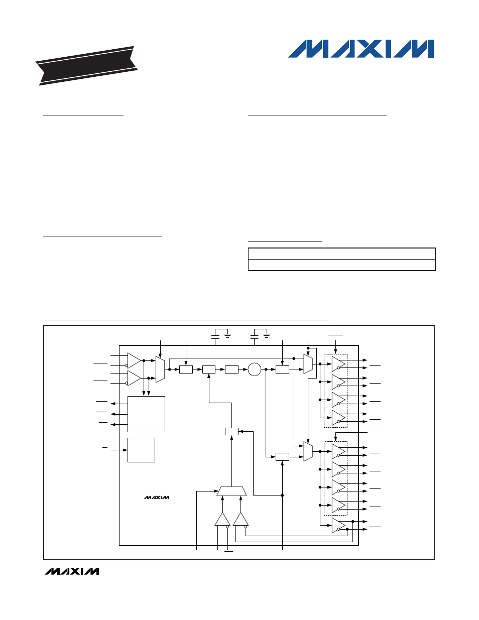
The MAX3671 is a low-jitter frequency synthesizer that
accepts two reference clock inputs and generates nine
phase-aligned outputs. The device features 40kHz jitter
transfer bandwidth, 0.3ps
RMS
(12kHz to 20MHz) inte-
grated phase jitter, and best-in-class power-supply
noise rejection (PSNR), making it ideal for jitter clean-
up, frequency translation, and clock distribution in
Gigabit Ethernet applications.
The MAX3671 operates from a single +3.3V supply and
typically consumes 400mW. The IC is available in an
8mm x 8mm, 56-pin TQFN package, and operates from
-40°C to +85°C.
Applications
Gigabit Ethernet Routers and Switches
Frequency Translation
Jitter Cleanup
Clock Distribution
Features
♦ Two Reference Clock Inputs: LVPECL
♦ Nine Phase-Aligned Clock Outputs: LVPECL
♦ Input Frequencies: 62.5MHz,125MHz, 250MHz,
312.5MHz
♦ Output Frequencies: 62.5MHz, 125MHz,
156.25MHz, 250MHz, 312.5MHz
♦ Low-Jitter Generation: 0.3ps
RMS
(12kHz to 20MHz)
♦ Clock Failure Indicator for Both Reference Clocks
♦ External Feedback Provides Zero-Delay Capability
♦ Low Output Skew: 20ps Typical
MAX3671
Low-Jitter Frequency Synthesizer
with Selectable Input Reference
________________________________________________________________
Maxim Integrated Products
1
Ordering Information
19-4437; Rev 0; 2/09
For pricing, delivery, and ordering information, please contact Maxim Direct at 1-888-629-4642,
or visit Maxim’s website at www.maxim-ic.com.
EVALUATION KIT
AVAILABLE
PART
TEMP RANGE
PIN-PACKAGE
MAX3671ETN+ -40
°C to +85°C 56
TQFN-EP*
SIGNAL QUALIFIER
AND
LOCK DETECT
POWER-ON
RESET
(POR)
IN0FAIL
IN1FAIL
LOCK
REFCLK0
REFCLK0
FB_IN
FB_SEL
FB_IN
REFCLK1
REFCLK1
MR
0
1
1
0
DIV M
DM
SEL_CLK
DA
DB
PFD
CP
DIV N
DIV A
DIV B
VCO
2.5GHz
62.5MHz
OUTA2
OUTA2
OUTA1
OUTA1
OUTA3
OUTA3
OUTA0
OUTB_EN
OUTA0
OUTA_EN
PLL_BYPASS
1
0
1
0
OUTB3
OUTB3
OUTB2
OUTB2
OUTB4
OUTB4
OUTB1
OUTB1
OUTB0
OUTB0
C
PLL
0.1
μF
C
REG
0.22
μF
MAX3671
Functional Diagram
+
Denotes a lead(Pb)-free/RoHS-compliant package.
*
EP = Exposed pad.
Pin Configuration and Typical Application Circuits appear at
end of data sheet.