Max105, Timing requirements – Rainbow Electronics MAX105 User Manual
Page 14
MAX105
and are internally buffered with a preamplifier to ensure
proper operation of the converter even with small-
amplitude sine-wave sources. The MAX105 was
designed for single-ended, low-phase noise sine wave
clock signals with as little as 500mV
P-P
amplitude
(-2dBm).
Single-Ended Clock (Sine-Wave Drive)
Excellent performance is obtained by AC- or DC-cou-
pling a low-phase noise sine-wave source into a single
clock input (
Figure 4). Essentially, the dynamic perfor-
mance of the converter is unaffected by clock-drive
power levels from -2dBm (500mV
p-p
clock signal ampli-
tude) to +10dBm (2V
P-P
clock signal amplitude). The
MAX105 dynamic performance specifications are
determined by a single-ended clock drive of -2dBm
(500mVp-p clock signal amplitude). To avoid saturation
of the input amplifier stage, limit the clock power level
to a maximum of +10dBm.
Differential Clock (Sine-Wave Drive)
The advantages of differential clock drive (Figure 5)
can be obtained by using an appropriate balun or
transformer to convert single-ended sine-wave sources
into differential drives. Refer to Single-Ended Clock
Inputs (Sine-Wave Drive) for proper input amplitude
requirements.
LVDS, ECL and PECL Clock
The innovative input architecture of the MAX105 clock
also allows these inputs to be driven by LVDS-, ECL-, or
PECL-compatible input levels, ranging from 500mV
p-p
to 2V
p-p
(Figure 6).
Timing Requirements
The MAX105 features a 6:12 demultiplexer, which
reduces the output data rate (including DREADY and
DOR signals) to one-half of the sample clock rate. The
Dual, 6-Bit, 800Msps ADC with On-Chip,
Wideband Input Amplifier
14
______________________________________________________________________________________
AGND
AGND
B
0
°
0
°
180
°
0
°
D
C
A
SIGNAL SOURCE
50
Ω
*TERMINATION OF THE UNUSED INPUT/OUTPUT (WITH 50
Ω TO AGND) ON A
BALUN IS RECOMMENDED IN ORDER TO AVOID UNWANTED REFLECTIONS.
CLK+,
INI+,
INQ+
CLK-,
INI-,
INQ-
100pF
100pF
50
Ω
50
Ω
AGND
50
Ω*
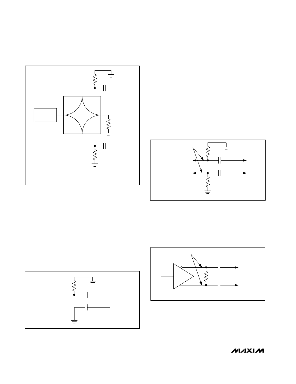
Figure 3. Single-Ended to Differential Conversion Using a Balun
AGND
AGND
FROM SIGNAL SOURCE
CLK+,
INI+,
INQ+
CLK-,
INI-,
INQ-
100pF
100pF
50
Ω
Figure 4. Single-Ended Clock Input With AC-Coupled Input
Drive (CLK, INI, INQ)
Figure 5. Differential AC-Coupled Input Drive (CLK, INI, INQ)
AGND
AGND
50
Ω TRANSMISSION LINES
TO 50
Ω-TERMINATED
SIGNAL SOURCE
OR BALUM
CLK+,
INI+,
INQ+
CLK-,
INI-,
INQ-
100pF
100pF
50
Ω
50
Ω
50
Ω TRANSMISSION LINES
LVDS LINE DRIVER
SIGNAL
SOURCE
INPUT
CLK+,
INI+,
INQ+
CLK-,
INI-,
INQ-
100pF
100pF
100
Ω
Figure 6. LVDS Input Drive (CLK, INI, INQ)