Max105, Internal reference, Lvds digital outputs – Rainbow Electronics MAX105 User Manual
Page 12

MAX105
signal-to-noise ratio (SNR) specifications will degrade.
The MAX105’s on-board, wide-bandwidth input ampli-
fiers (I&Q) reduce this effect significantly, allowing pre-
cise digitizing of fast analog data at high conversion
rates. The input amplifiers buffer the input signal and
allow a full-scale signal input range of ±400mV
(800mV
p-p
).
Internal Reference
The MAX105 features an integrated, buffered +2.5V
precision bandgap reference. This reference is internal-
ly scaled to match the analog input range specification
of ±400mV. The data converter’s reference output
(REF) can source up to 500µA. REF should be buffered,
if used to supply external devices.
LVDS Digital Outputs
The MAX105 provides data in two’s complement format
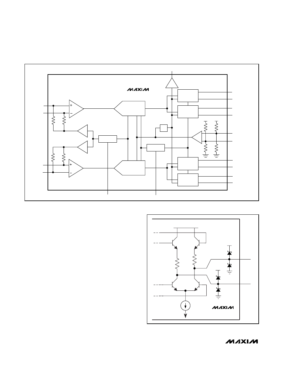
to differential LVDS outputs. A simplified circuit
schematic of the LVDS output cells is shown in
Figure
2. All LVDS outputs are powered from separate I-chan-
nel OV
CC
I and Q-channel OV
CC
Q (Q-channel) power
supplies, which may be operated at +3.3V ±10%. The
Dual, 6-Bit, 800Msps ADC with On-Chip,
Wideband Input Amplifier
Figure 1. MAX105 Flash Converter Architecture
INI-
INI+
2k
Ω
CLK+
AV
CC
CLK-
P0I+/P0I-
DREADY+/DREADY-
DOR+/DOR-
P5I+/P5I-
A0I+/A0I-
A5I+/A5I-
P0Q+/P0Q-
P5Q+/P5Q-
A0Q+/A0Q-
A5Q+/A5Q-
10k
Ω
10k
Ω
CM BUFFER
CM BUFFER
REFERENCE
PRIMARY
DATA PORT
P0I-P5I
AUXILIARY
DATA PORT
A0I-A5I
PRIMARY
DATA PORT
P0Q-P5Q
AUXILIARY
DATA PORT
A0Q-A5Q
I ADC
1:2
REF
MAX105
INQ-
INQ+
2k
Ω
PRE-AMP
Q ADC
REF
REF
DOR
PRE-AMP
MAX105
P0I+ - P5I+
A0I+ - A5I+
P0I- - P5I-
A0I- - A5I-
OV
CC
I
OV
CC
I
OV
CC
I
55
Ω
55
Ω
Figure 2. Simplified LVDS Output Model
12
______________________________________________________________________________________
