Detailed description – Rainbow Electronics MAX871 User Manual
Page 5
_______________Detailed Description
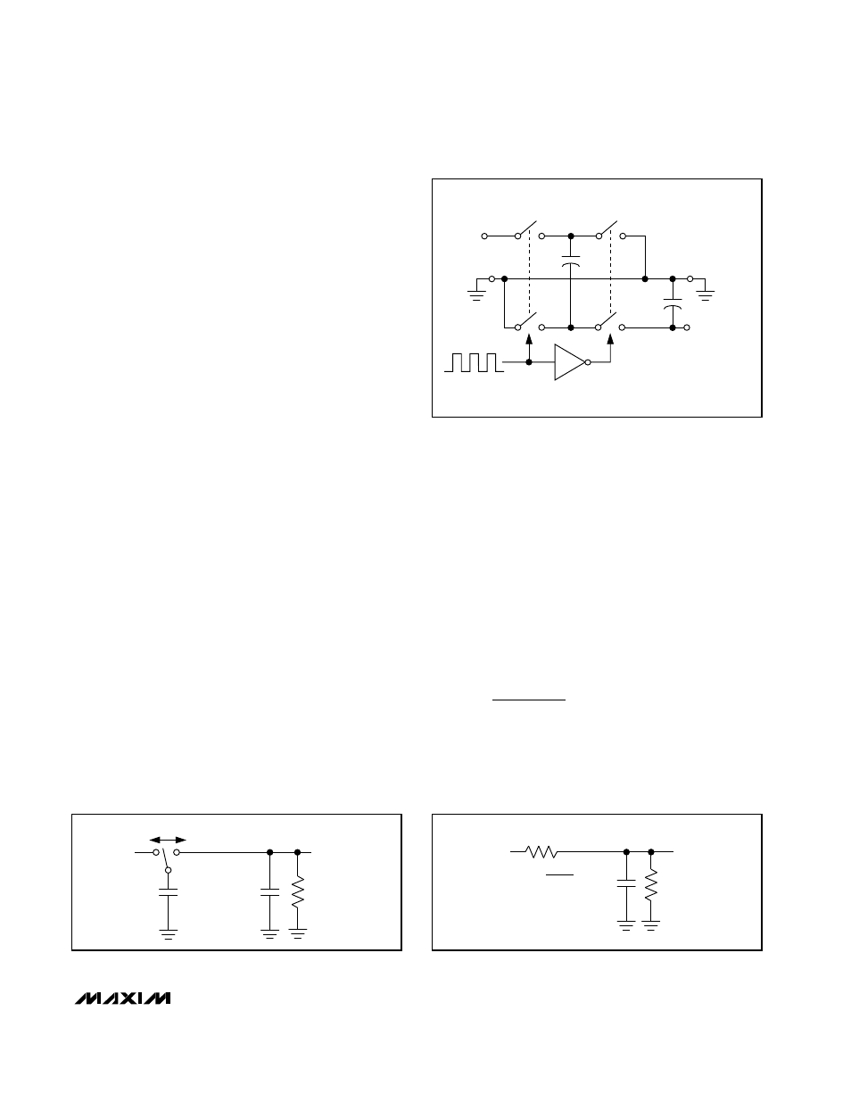
The MAX870/MAX871 capacitive charge pumps invert
the voltage applied to their input. For highest perfor-
mance, use low equivalent series resistance (ESR)
capacitors (e.g., ceramic).
During the first half-cycle, switches S2 and S4 open,
switches S1 and S3 close, and capacitor C1 charges to
the voltage at IN (Figure 2). During the second half-
cycle, S1 and S3 open, S2 and S4 close, and C1 is level
shifted downward by V
IN
volts. This connects C1 in par-
allel with the reservoir capacitor C2. If the voltage across
C2 is smaller than the voltage across C1, then charge
flows from C1 to C2 until the voltage across C2 reaches
-V
IN
. The actual voltage at the output is more positive
than -V
IN
, since switches S1–S4 have resistance and the
load drains charge from C2.
Charge-Pump Output
The MAX870/MAX871 are not voltage regulators: the
charge pump’s output source resistance is approxi-
mately 20
Ω
at room temperature (with V
IN
= +5V), and
V
OUT
approaches -5V when lightly loaded. V
OUT
will
droop toward GND as load current increases. The
droop of the negative supply (V
DROOP-
) equals the cur-
rent draw from OUT (I
OUT
) times the negative convert-
er’s source resistance (RS-):
V
DROOP-
= I
OUT
x RS-
The negative output voltage will be:
V
OUT
= -(V
IN
– V
DROOP-
)
Efficiency Considerations
The power efficiency of a switched-capacitor voltage
converter is affected by three factors: the internal loss-
es in the converter IC, the resistive losses of the pump
capacitors, and the conversion losses during charge
transfer between the capacitors. The total power loss is:
The internal losses are associated with the IC’s internal
functions, such as driving the switches, oscillator, etc.
These losses are affected by operating conditions such
as input voltage, temperature, and frequency.
The next two losses are associated with the voltage
converter circuit’s output resistance. Switch losses
occur because of the on-resistance of the MOSFET
switches in the IC. Charge-pump capacitor losses
occur because of their ESR. The relationship between
these losses and the output resistance is as follows:
where f
OSC
is the oscillator frequency. The first term is
the effective resistance from an ideal switched-
capacitor circuit. See Figures 3a and 3b.
Σ
P
= P
+ P
+ P
+ P
LOSS
INTERNAL LOSSES
SWITCH LOSSES
PUMP CAPACITOR LOSSES
CONVERSION LOSSES
MAX870/MAX871
Switched-Capacitor Voltage Inverters
_______________________________________________________________________________________
5
S1
IN
S2
S3
S4
C1
C2
V
OUT
= -(V
IN
)
Figure 2. Ideal Voltage Inverter
V+
C1
f
C2
R
L
V
OUT
Figure 3a. Switched-Capacitor Model
R
EQUIV
=
R
EQUIV
V
OUT
R
L
1
V+
f
×
C1
C2
Figure 3b. Equivalent Circuit
P
+P
= I
x R
PUMP CAPACITOR LOSSES
CONVERSION LOSSES
OUT
2
OUT
R
f
x C
R
ESR
ESR
OUT
OSC
SWITCHES
C
C
≅
( )
+
+
+
1
1
2
4
1
2