Adjusting the regulation set point, Automatic input disable, In_offset) / (4 x v – Rainbow Electronics MAX1804 User Manual
Page 7
MAX1804
External Four-Input Feedback Integrator for
Power Supplies
_______________________________________________________________________________________
7
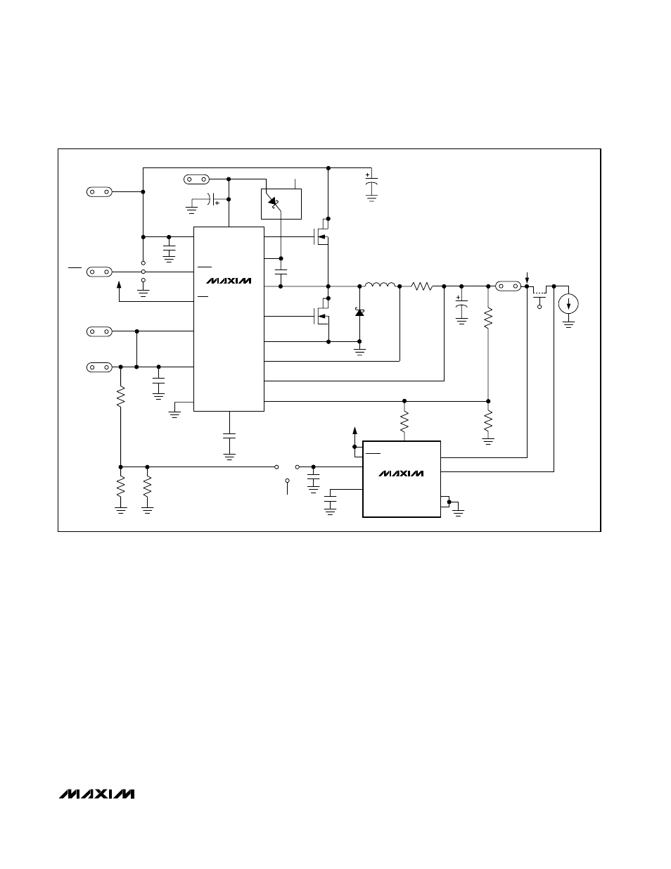
The MAX1804 only sinks current at OUT (Figure 4). The
maximum sink current and maximum regulator voltage
increase are limited by the minimum guaranteed OUT
current of 10µA. The maximum regulator output voltage
increase can be further limited by including a resistor
between OUT and the feedback point of the regulator.
If any of the IN_ inputs fall to 90% of the regulation set
point, they are automatically disabled and OUT contin-
ues to regulate according to the lowest remaining
active input. See Automatic Input Disable.
Adjusting the Regulation Set Point
The MAX1804 monitors the voltage at the IN1–IN4
sense inputs and regulates the lowest active input to
four times the reference voltage at ADJ. The IN1–IN4
regulation set point is calculated as:
V
IN_
= 4
✕
V
ADJ
The total error in the MAX1804 regulation set point is:
total percentage error = [(IN_scale factor x V
ADJ
+
IN_offset) / (4 x V
ADJ
)] x 100%
The maximum IN_ voltage is 5.5V. Use the MAX1804 for
higher output voltages by using an external divider to
divide down the desired output voltage at the IN1–IN4
pins. Since the IN_ input bias current is fairly high (1.5µA
typ), choose the resistive divider accordingly.
Automatic Input Disable
The MAX1804 has an input buffer stage that monitors
the sense inputs (IN1–IN4) and connects the lowest to
its internal integrator (Figure 4). Each input is com-
pared to 90% of the set point. If the input falls below
this value, the input buffer is disabled and the output
voltage is adjusted according to the lowest of the
remaining active inputs (see Automatic Input Disable in
Typical Operating Characteristics). If all four sense
4.5V TO 28V
VIN
VOUT
SHDN
SYNC
REF
3
10
16
1
2
3
14
11
15
13
12
8
9
7
DH
BST
VL
LX
DL
PGND
CSH
CSL
FB
6
6
4
3
1
5
8
2
7
2
5
3
4
1
V+
SHDN
N1B
IRF7303
D1
CMPSH-3
C4
0.1
µF
N1A
IRF7303
D2
MBR0530
SKIP
SYNC
REF
GND
1M
SS
JU3
2
JU4
EXT
REF
COMP
ADJ
IN2
IN3
IN4
IN1
OUT
V+
VL
C6
0.01
µF
0.01
µF
C5
0.33
µF
100k
100k
JU2
JU1
3
VL
VL
2
3
1
C2
0.1
µF
C1
22
µF
35V
C7
220
µF
10V
R
TOP
91k
1%
5V± 5%
PFET
I
LOAD
R
BOTTOM
100k
1%
562k
C3
4.7
µF
16V
L1
15
µH
R1
0.033
Ω
1%
2
U1
MAX1653
MAX1804
SHDN
Figure 2. Application Circuit with Step-Down Regulator