Rainbow Electronics MAX1804 User Manual
Page 2
MAX1804
External Four-Input Feedback Integrator for
Power Supplies
2
_______________________________________________________________________________________
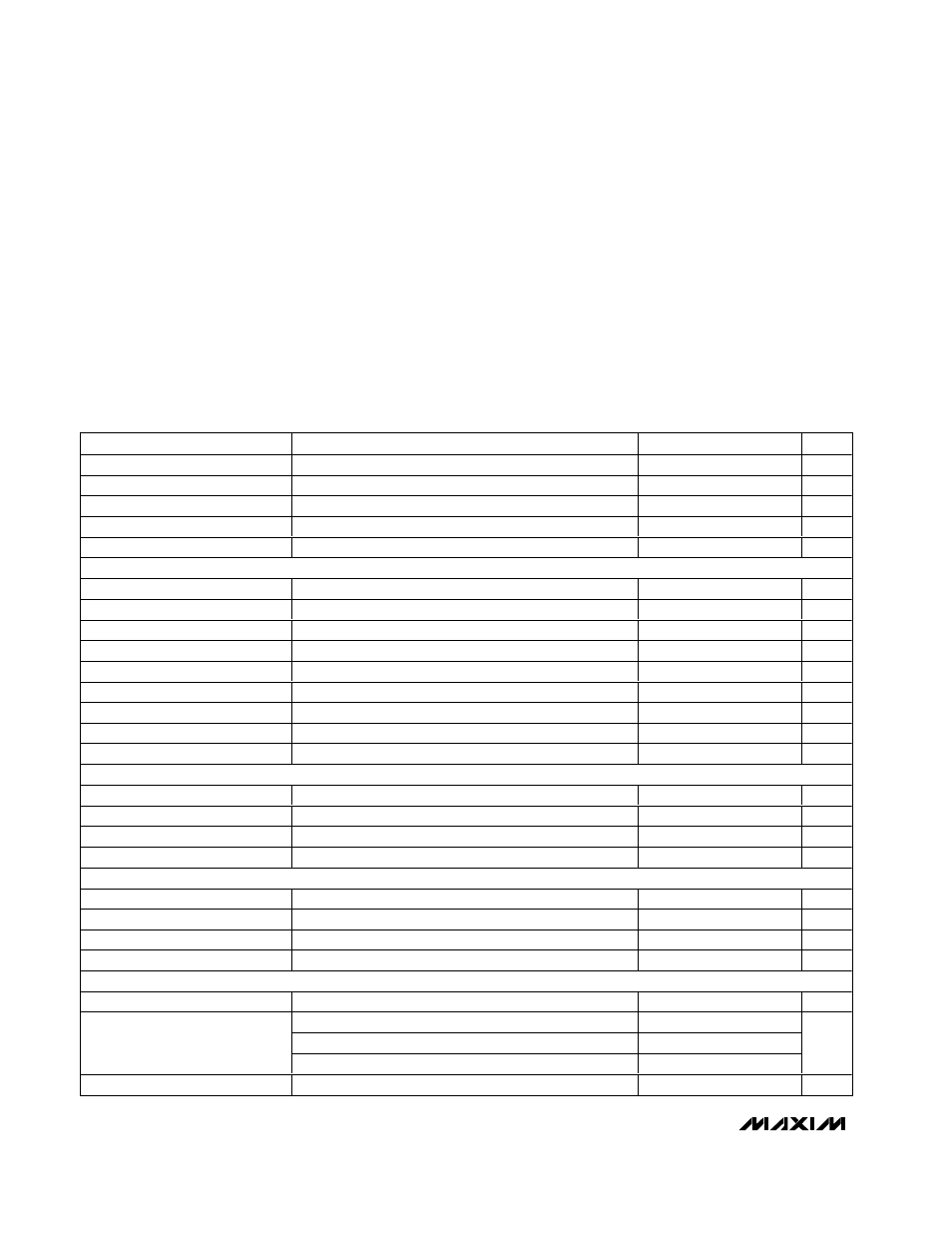
ABSOLUTE MAXIMUM RATINGS
ELECTRICAL CHARACTERISTICS
(T
A
= 0
°C to +85°C, V
V
+ = 3.3V, V
ADJ
= 1.2V, V
OUT
= 2V, C
V
+ = 0.1µF, C
COMP
= 470pF. Typical values are at T
A
= +25
°C, unless
otherwise noted.)
Stresses beyond those listed under “Absolute Maximum Ratings” may cause permanent damage to the device. These are stress ratings only, and functional
operation of the device at these or any other conditions beyond those indicated in the operational sections of the specifications is not implied. Exposure to
absolute maximum rating conditions for extended periods may affect device reliability.
V+, IN1, IN2, IN3, IN4, OUT, ADJ, SHDN to GND...…-0.3V, +6V
COMP to GND ....................................................-0.3V, V+ +0.3V
Continuous Power Dissipation (T
A
= +70
°C)
10-Pin µMAX (derate 8.3mW/
°C above +70°C) ..........667mW
Operating Temperature Extended Range ...........-40°C to +85
°C
Junction Temperature ..................…………………………+150
°C
Storage Temperature Range .……...……………-65°C to +165
°C
Lead Temperature (soldering, 10s) .................................+300
°C
PARAMETER
CONDITIONS
MIN
TYP
MAX
U N IT S
Supply Voltage Range (V+)
2.7
5.5
V
Shutdown Supply Current (V+)
SHDN = GND
0.01
1
µA
Quiescent Supply Current (V+)
SHDN = V+
25
35
µA
UVLO Threshold, Rising
2.5
2.6
V
UVLO Threshold, Falling
2.3
2.4
V
INTEGRATOR INPUTS IN1–IN4
IN_ Voltage Range
0
5.5
V
IN_ Offset
V
V+
= 2.7V to 5.5V
-15
15
mV
IN_ Scale Factor
V
ADJ
= 0.7V to 1.4V
3.988
4.000
4.016
V/V
IN_ Transconductance
V
IN_
= 4.75V to 4.85V, V
COMP
= 1.3V
12
30
48
µS
IN_ Bias Current
V
IN_
= 4.8V
1.5
2.7
µA
IN_ Shutdown Current
SHDN = GND
0.2
µA
IN_ Leakage Current
V
V+
= 0, V
SHDN
= 0
0.2
µA
IN_ Disable Threshold
V
ADJ
= 0.7V to 1.4V, V
ADJ
x 4, falling edge
87
90
93
%
IN_ Disable Threshold Hysteresis
V
ADJ
= 0.7V to 1.4V, rising edge
50
mV
ADJ INPUT
ADJ Voltage Range
0.7
1.4
V
ADJ Bias Current
-20
20
nA
ADJ Shutdown Current
SHDN = GND
0.2
µA
ADJ Leakage Current
V
V+
= 0, V
SHDN
= 0
0.2
µA
COMP OUTPUT
COMP Source Current
V
COMP
= 1.3V, V
IN_
= 4.6V
1.6
2.0
2.4
µA
COMP Sink Current
V
COMP
= 1.3V, V
IN_
= 5.0V
1.6
2.0
2.4
µA
COMP Output Voltage Low
Sink 1
µA, V
IN_
= 5.0V
0.2
V
COMP Output Voltage High
Source 1
µA, V
IN_
= 4.6V
2.4
V
OUT OUTPUT
OUT Output Voltage Low
I
OUT
= 10
µA, V
IN_
= 4.6V
0.2
V
V
SHDN
= 0
0.1
V
V+
= 0
0.1
OUT Output Leakage Current
V
IN_
= 5.0V
0.1
µA
OUT Transconductance
V
COMP
= 1V to 2V
4
10
22
µS