Max1759 buck/boost regulating charge pump in µmax, Detailed description, Design procedure – Rainbow Electronics MAX1759 User Manual
Page 6

MAX1759
Buck/Boost Regulating
Charge Pump in µMAX
6
_______________________________________________________________________________________
Detailed Description
The MAX1759’s unique charge-pump architecture
allows the input voltage to be higher or lower than the
regulated output voltage. Internal circuitry senses V
IN
and V
OUT
and determines whether V
IN
must be
stepped up or stepped down to produce the regulated
output. When V
IN
is lower than V
OUT
, the charge pump
operates as a regulated step-up voltage doubler. When
V
IN
is higher than V
OUT
, the charge pump operates as
a step-down gated switch.
In voltage step-down mode (i.e., the input voltage is
greater than the output voltage) with a light load, the
controller connects CXN to PGND, and shuttles charge
to the output by alternately connecting CXP from IN to
OUT (see Figures 1 and 2). Although V
IN
is greater than
V
OUT
, this scheme may not allow the MAX1759 to regu-
late the output under heavy loads. In this case, the
MAX1759 will automatically switch to step-up mode. In
step-up mode, the output is kept in regulation by modu-
lating the charge delivered by the transfer capacitor
(C
X
) to the load (see Figure 2). When lightly loaded, the
charge pump switches only as necessary to supply the
load, resulting in low quiescent current. Output voltage
ripple does not increase with light loads.
Shutdown Mode
Driving SHDN low places the MAX1759 in shutdown
mode. This disables the charge-pump switches, oscil-
lator, and control logic, reducing quiescent current to
1µA. The output is high impedance in shutdown and is
disconnected from the input. The POK output is high
impedance in shutdown.
Undervoltage Lockout
The MAX1759 undervoltage lockout feature deactivates
the device when the input voltage falls below 1V.
Power-OK Output
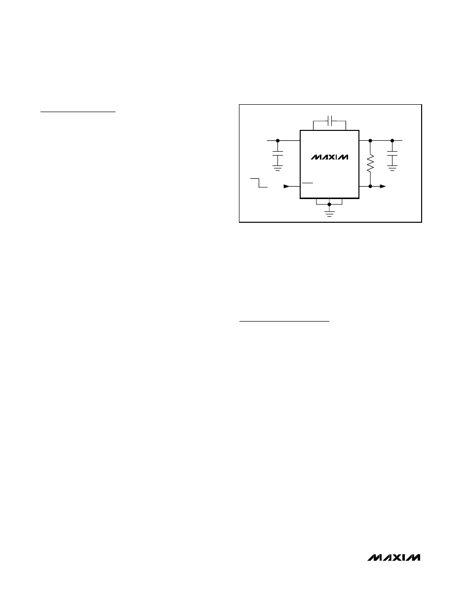
POK is an open-drain output that sinks current when
the regulator feedback voltage falls below 1.1V. The
feedback voltage can be either the internal resistor-
divider feedback voltage when in fixed output mode
(FB tied to GND) or an external feedback voltage from
an external resistive divider in adjustable output mode.
A 10k
Ω to 1MΩ pull-up resistor from POK to OUT may
be used to provide a logic output. Connect POK to GND
or leave unconnected if not used.
Soft-Start and Short-Circuit Protection
The MAX1759 features foldback short-circuit protec-
tion. This circuitry provides soft-start by limiting inrush
current during startup and limits the output current to
110mA (typ) if the output is short-circuited to ground.
Thermal Shutdown
The MAX1759 features thermal shutdown with tempera-
ture hysteresis. When the die temperature exceeds
160°C, the device shuts down. When the die cools by
20°C, the MAX1759 turns on again. If high die tempera-
ture is caused by output overload and the load is not
removed, the device will turn off and on, resulting in a
pulsed output.
Design Procedure
Setting the Output Voltage
The MAX1759 dual-mode feedback controller selects
between the internally set 3.3V regulated output or an
external resistive divider that allows adjustment of the
output voltage from 2.5V to 5.5V. Connect FB to GND
for a regulated 3.3V output. For an adjustable output,
connect a resistive divider between OUT and GND. To
ensure feedback-loop stability and to minimize error due
to FB pin bias currents, the resistive divider current
should be approximately 15µA. In the following equa-
tion, choose R2 in the 50k
Ω to 100kΩ range, and calcu-
late R1 from the following formula (Figure 3):
R1 = R2 [(V
OUT
/ V
FB
) - 1]
and
V
OUT
= V
FB
(R1 + R2) / R2
where V
OUT
is the desired output voltage from 2.5V to
5.5V, and V
FB
is the internal regulation voltage, nomi-
nally 1.235V.
The circuit of Figure 3 generates a regulated 2.5V, using
external standard 1% resistor values. Surface-mount
resistors should be placed close to the MAX1759, less
than 5mm away from FB (see the PC Board Layout
section).
0.33
µF
IN
+1.6V TO +5.5V
OUT
3.3V AT 100mA
10
µF
ON
OFF
10
µF
100k
POWER OK
OUT
POK
IN
CXN
CXP
PGND
GND
FB
SHDN
MAX1759
Figure 1. Typical Application Circuit
