Max1759 buck/boost regulating charge pump in µmax, Typical operating characteristics (continued), Pin description – Rainbow Electronics MAX1759 User Manual
Page 5
MAX1759
Buck/Boost Regulating
Charge Pump in µMAX
_______________________________________________________________________________________
5
Typical Operating Characteristics (continued)
(Circuit of Figure 1, C
IN
= 10µF, C
X
= 0.33µF, C
OUT
= 10µF, V
OUT
= 3.3V, V
IN
= 2.5V, T
A
= +25°C, unless otherwise noted.)
NAME
FUNCTION
1
POK
Open-Drain Power-OK Output. POK is high impedance when output voltage is in regulation. POK sinks current
when V
FB
falls below 1.1V. Connect a 10k
Ω to 1MΩ pull-up resistor from POK to V
OUT
for a logic signal.
Ground POK or leave unconnected if not used. POK is high impedance in shutdown.
2
SHDN
Shutdown Input. Drive high for normal operation; drive low for shutdown mode. OUT is high impedance in
shutdown.
PIN
3, 4
IN
Input Supply. Connect both pins together and bypass to GND with a ceramic capacitor (see Capacitor
Selection section).
5
GND
Ground. Connect GND to PGND with a short trace.
9
OUT
Power Output. Bypass to GND with an output filter capacitor.
8
CXP
Positive Terminal of the Charge-Pump Transfer Capacitor
7
CXN
Negative Terminal of the Charge-Pump Transfer Capacitor
6
PGND
Power Ground. Charge-pump current flows through this pin.
10
FB
Dual-Mode Feedback. Connect FB to GND for 3.3V output. Connect to an external resistor divider to adjust
the output voltage from 2.5V to 5.5V.
Pin Description
1
2
-4.2V
-2.5V
100
µs/div
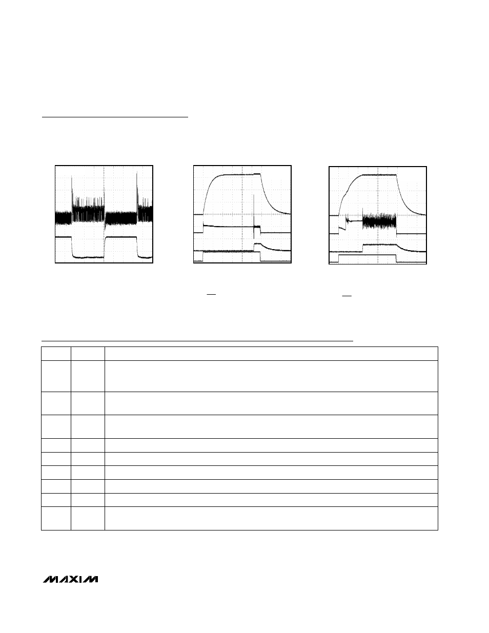
LINE-TRANSIENT RESPONSE
MAX1759 toc10
CH1: V
OUT
, 20mV/div, AC-COUPLED
CH2: V
IN
, 1V/div, AC-COUPLED
R
LOAD
= 33
Ω
1
2
3
4
500
µs/div
TURN-ON/OFF RESPONSE
(V
IN
= 4.2V)
MAX1759 toc11
CH1: V
OUT
,1V/div
CH2: I
IN
, 200mA/div
CH3: V
POK
, 5V/div
CH4: V
SHDN
, 5V/div
R
LOAD
= 33
Ω
V
IN
= 4.2V
1
2
3
4
500
µs/div
TURN-ON/OFF RESPONSE
(V
IN
= 2.5V)
MAX1759 toc12
CH1: V
OUT
,1V/div
CH2: I
IN
, 200mA/div
CH3: V
POK
, 5V/div
CH4: V
SHDN
, 5V/div
R
LOAD
= 33
Ω
V
IN
= 2.5V