Max1759 buck/boost regulating charge pump in µmax – Rainbow Electronics MAX1759 User Manual
Page 2

MAX1759
Buck/Boost Regulating
Charge Pump in µMAX
2
_______________________________________________________________________________________
ABSOLUTE MAXIMUM RATINGS
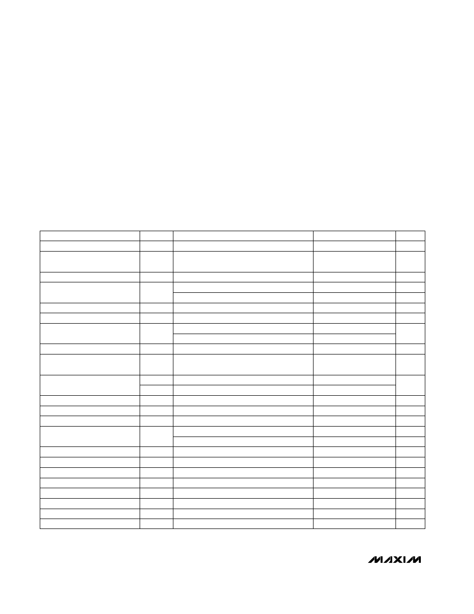
ELECTRICAL CHARACTERISTICS
(Circuit of Figure 1, V
IN
= V
SHDN
= 2V, FB = PGND = GND, C
IN
= 10µF, C
X
= 0.33µF, C
OUT
= 10µF, T
A
= 0°C to +85°C, unless oth-
erwise noted. Typical values are at T
A
= +25°C.)
Stresses beyond those listed under “Absolute Maximum Ratings” may cause permanent damage to the device. These are stress ratings only, and functional
operation of the device at these or any other conditions beyond those indicated in the operational sections of the specifications is not implied. Exposure to
absolute maximum rating conditions for extended periods may affect device reliability.
IN, OUT, FB, POK, SHDN to GND............................-0.3V to +6V
PGND to GND.....................................................................±0.3V
CXN to GND ................................................-0.3V to (V
IN
+ 0.3V)
CXP to GND................-0.3V to (the greater of V
IN
or V
OUT
) + 1V
OUT Short to GND .........................................................Indefinite
Continuous Power Dissipation (T
A
= +70°C)
10-Pin µMAX (derate 5.6mW/°C above +70°C) .........444mW
Operating Temperature Range .......................... -40°C to +85°C
Junction Temperature ......................................................+150°C
Storage Temperature Range .............................-65°C to +150°C
Lead Temperature (soldering, 10s) ................................ +300°C
I
LOAD,MAX
Thermal Shutdown Hysteresis
20
°C
Efficiency
90
%
V
IN
= 3.6V, I
LOAD
= 10mA
PARAMETER
SYMBOL
MIN
TYP
MAX
UNITS
Transient Load Current
200
mA
Maximum Output Current
100
mA
3.17
3.3
3.43
Output Voltage
V
OUT
3.17
3.3
3.43
V
Quiescent Supply Current
I
Q
50
90
85
180
µA
Shutdown Supply Current
I
Q,SHDN
1
5
µA
Leakage Current into OUT in
Shutdown
1
5
µA
Input Undervoltage Lockout
Voltage
Input Voltage Range
V
IN
1.6
5.5
V
V
UVLO
0.6
1.0
1.4
V
Output Voltage Adjustment Range
2.5
5.5
V
SHDN Logic Input Voltage
V
IL
0.25
·
V
IN
V
V
IH
0.7
·
V
IN
SHDN Input Leakage Current
I
SHDN
-1
1
µA
FB Regulation Voltage
V
FB
1.205
1.235
1.265
V
FB Input Current
25
200
nA
FB Dual-Mode Threshold
100
50
mV
200
100
mV
POK Trip Voltage
1.0
1.1
1.2
V
POK Output Low Voltage
V
OL
5
100
mV
POK Leakage Current
0.01
0.2
µA
Switching Frequency
f
OSC
1.2
1.5
1.8
MHz
Output Short-Circuit Current
110
mA
Thermal Shutdown Temperature
160
°C
CONDITIONS
1.6V
≤ V
IN
≤ 5.5V
I
LOAD
≤ 100mA (RMS)
1.6V
≤ V
IN
≤ 5.5V
2.5V
≤ V
IN
≤ 5.5V
2.5V
≤ V
IN
≤ 5.5V, 1mA ≤ I
LOAD
≤ 100mA
2V
≤ V
IN
≤ 5.5V, 1mA ≤ I
LOAD
≤ 50mA
V
IN
= V
SHDN
= 4V, V
FB
= 0, stepping down
V
IN
= V
SHDN
= 2V, V
FB
= 0, stepping up
V
SHDN
= 5.5V
V
IN
= 1.65V, V
OUT
= 3.3V
1.6V
≤ V
IN
≤ 5.5V, V
SHDN
= 0
V
IN
= 2V, V
OUT
= 3.3V, V
SHDN
= 0
V
FB
= 1.27V
Internal feedback
External feedback
Falling edge at FB
I
SINK
= 0.5mA, V
IN
= 2V
V
POK
= 5.5V, V
FB
= 1.27V
1.6V
≤ V
IN
≤ 5.5V
1.6V
≤ V
IN
≤ 5.5V, V
FB
= 1V
V
OUT
= 0, 2.5V
≤ V
IN
≤5.5V, foldback current limit
Rising temperature
