Rainbow Electronics MAX786 User Manual
Page 15

MAX786
Dual-Output Power-Supply
Controller for Notebook Computers
______________________________________________________________________________________
15
Be sure to select output capacitors that satisfy
both
the minimum capacitance and maximum ESR require-
ments. To achieve the low ESR required, it may be
appropriate to use a capacitance value 2 or 3 times
larger than the calculated minimum.
The output ripple in continuous-current mode is:
V
OUT(RPL)
= I
LPP(MAX)
x (ESR
CF
+ 1/(2 x
π
x f x C
F
) ).
In idle-mode, the ripple has a capacitive and resistive
component:
(4) (10
-4
) (L)
V
OUT(RPL)
(C) = ——————— x
(R
CS
2
) (C
F
)
1 1
(
——— + —————
)
Volts
V
OUT
V
IN
- V
OUT
(0.02) (ESR
CF
)
V
OUT(RPL)
(R) = ———————- Volts
R
CS
The total ripple, V
OUT(RPL)
, can be approximated as
follows:
if V
OUT(RPL)
(R) < 0.5 V
OUT(RPL)
(C),
then V
OUT(RPL)
= V
OUT(RPL)
(C),
otherwise, V
OUT(RPL)
= 0.5 V
OUT(RPL)
(C) +
V
OUT(RPL)
(R).
Diodes D1 and D3
Use 1N5819s or similar Schottky diodes. D1 and D3
conduct only about 3% of the time, so the 1N5819’s
1A current rating is conservative. The voltage rating
of D1 and D3 must exceed the maximum input supply
v o l t a g e f r o m t h e b a t t e r y . T h e s e d i o d e s m u s t
be Schottky diodes to prevent the lossy MOSFET
body diodes from turning on, and they must be
placed physically close to their associated synchro-
nous rectifier MOSFETs.
Soft-Start Capacitors (C8, C9)
A capacitor connected from GND to either SS pin
causes that supply to ramp up slowly. The ramp time to
full current limit, t
SS
, is approximately 1ms for every nF
of capacitance on SS_, with a minimum value of 10µs.
Typical capacitor values are in the 10nF to 100nF
range; a 5V rating is sufficient.
Because this ramp is applied to the current-limit circuit,
the actual time for the output voltage to ramp up
depends on the load current and output capacitor
value. Using Figure 1’s circuit with a 2A load and no SS
capacitor, full output voltage is reached about 600µs
after ON_ is driven high.
Boost Capacitors (C4, C5)
Capacitors C4 and C5 store the boost voltage and pro-
vide the supply for the DH3 and DH5 drivers. Use 0.1µF
and place each within 10mm of the BST_ and LX_ pins.
Boost Diodes (D1A, D1B)
Use high-speed signal diodes; e.g., 1N4148 or
equivalent.
Bypass Capacitors
Input Filter Capacitors (C1, C10)
Use at least 3µF/W of output power for the input filter
capacitors, C1 and C10. They should have less than
150m
Ω
ESR, and should be located no further than
10mm from N1 and N2 to prevent ringing. Connect the
negative terminals directly to PGND. Do not exceed the
surge current ratings of input bypass capacitors.
Shutdown Mode
Shutdown (SHDN = low) forces both PWMs off and dis-
ables the REF output and both comparators (Q1 = Q2
= 0V). Supply current in shutdown mode is typically
25µA. The VL supply remains active and can source
25mA for external loads. Note that the VL load capabili-
ty is higher in shutdown and standby modes than when
the PWMs are operating (25mA vs. 5mA). Standby
mode is achieved by holding ON3 and ON5 low while
SHDN is high. This disables both PWMs, but keeps VL,
REF, and the precision comparators alive. Supply current
in standby mode is typically 70µA.
MAX786
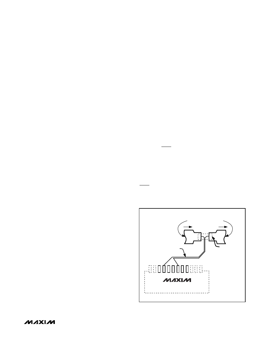
KELVIN SENSE TRACES
SENSE RESISTOR
MAIN CURRENT PATH
FAT, HIGH-CURRENT TRACES
Figure 5. Kelvin Connections for the Current-Sense Resistors
