Pin description – Rainbow Electronics MAX1873 User Manual
Page 8
MAX1873
Simple Current-Limited Switch-Mode
Li+ Charger Controller
8
_______________________________________________________________________________________
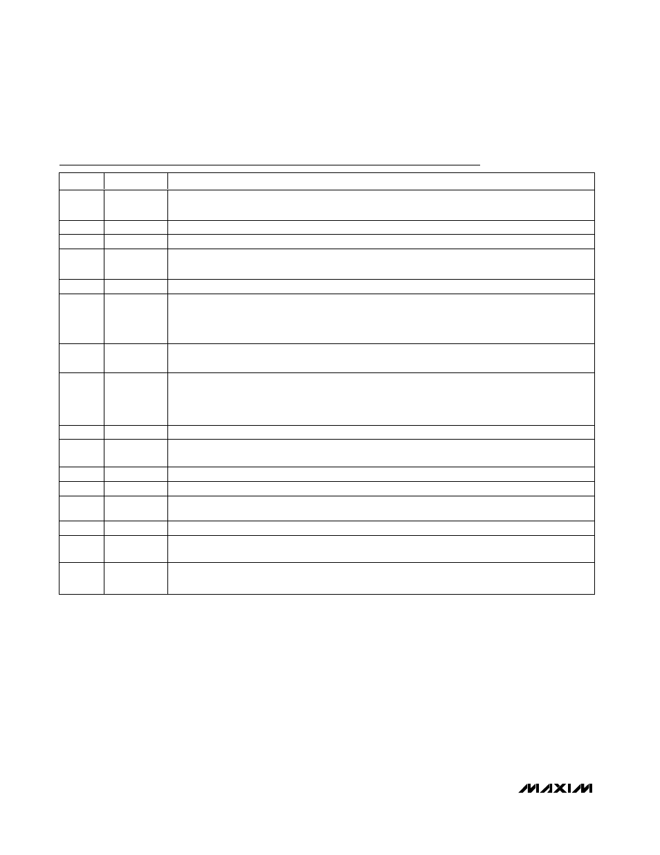
Pin Description
PIN
NAME
FUNCTION
1
CSSN
Source Current-Sense Negative Input. Connect a current-sense resistor between CSSP and CSSN to
limit total current drawn from the input source. To disable input current sensing, connect CSSN to CSSP.
2
CSSP
Source Current-Sense Positive Input. Also used for input source undervoltage sensing.
3
CCS
Input-Source-Current Regulation Loop Compensation Point
4
CCV
Battery Regulation Voltage Control-Loop Compensation Point. Pulling CCV high (to VL) through a 1.5k
Ω
resistor disables the voltage control loop for charging NiCd or NiMH batteries.
5
CCI
Battery Charge Current Control-Loop Compensation Point
6
ICHG/EN
Battery Charging Current Adjust/Shutdown Input. This pin can be connected to a resistive-divider
between REF and GND to adjust the charge current sense threshold between CSB and BATT. When
ICHG/EN is connected to REF, the CSB-BATT threshold is 200mV. Pull ICHG/EN low (below 500mV) to
disable charging and reduce the supply current to 5µA.
7
IOUT
Charge Current Monitor Output. Analog Voltage Output that is proportional to charging current. V
IOUT
= 20 (V
CSB
- V
BATT
) or 4V for a 200mV current-sense voltage (maximum load capacitance = 5nF).
8
VADJ
Battery Regulation Voltage Adjust. Set the battery regulation voltage from 3.979V per cell to 4.421V per
cell with 1% resistors. Output accuracy remains better than 0.75% even with 1% adjusting resistors
due to reduced adjustment range. For 4.2V, the voltage-divider resistors must be equal value
(nominally 100k
Ω each).
9
REF
4.2V Reference Voltage Output. Bypass to GND with a 1µF ceramic capacitor.
10
BATT
Battery Voltage-Sense Input and Battery Current-Sense Negative Input. Bypass to GND with a 68µF for
MAX1873R, 47µF for MAX1873S, and 33µF for MAX1873T. Use capacitors with ESR < 1
Ω.
11
CSB
Battery Current-Sense Positive Input
12
GND
Ground
13
VH
Internal VH Regulator. VH internally supplies power to the EXT driver. Connect a 0.22µF ceramic
capacitor between VH and DCIN.
14
EXT
Drive Output for External PFET. EXT swings from V
DCIN
to V
DCIN
- 5V.
15
DCIN
Power-Supply Input. DCIN is the input supply for charger IC. Bypass to GND with a 0.22µF ceramic
capacitor.
16
VL
Internal VL Regulator. VL powers the MAX1873’s control logic at 5.4V. Bypass to GND with a 2.2µF or
larger ceramic capacitor.