Applications information, Chip information, Pin configuration – Rainbow Electronics MAX1873 User Manual
Page 13

where C
OUT
is the total output capacitance, V
REF
is the
reference voltage (4.2V), V
BATT
is the maximum battery
regulation voltage (typically 4.2V per cell), V
DCIN (MIN)
is the minimum source-input voltage, and R
CSB
is the
current-sense resistor (68m
Ω for 3A charging current)
from CSB to BATT.
The maximum output capacitor ESR allowed for stability is:
where R
ESR
is the output capacitor ESR.
Compensation Components
The three regulation loops: input current limit, charging
current limit, and charging voltage limit are compensat-
ed separately using the CCS, CCI, and CCV pins,
respectively.
The charge-current loop error-amplifier output is
brought out at CCI. Likewise, the source-current error-
amplifier output is brought out at CCS. 47nF capacitors
to ground at CCI and CCS compensate the current
loops in most charger designs. Raising the value of
these capacitors reduces the bandwidth of these loops.
The voltage-regulating loop error-amplifier output is
brought out at CCV. Compensate this loop by connect-
ing a capacitor in parallel with a series resistor-capaci-
tor from CCV to GND. Recommended values are shown
in Figure 1.
Applications Information
VL, VH, and REF Bypassing
The MAX1873 uses two internal linear regulators to
power internal circuitry. The outputs of the linear regu-
lators are at VL and VH. VL powers the internal control
circuitry while VH powers the MOSFET gate driver. VL
may also power a limited amount of external circuitry,
as long as its maximum current (3mA) is not exceeded.
A 2.2µF bypass capacitor is required from VL to GND
to ensure stability. A 0.22µF capacitor is required from
VH to DCIN. A 1µF bypass capacitor is required
between REF and GND to ensure that the internal 4.2V
reference is stable. In all cases, use low-ESR ceramic
capacitors.
Charging NiMH and NiCd Cells
The MAX1873 may be used in multichemistry chargers.
When charging NiMH or NiCd cells, pull CCV high (to
VL) with a 1.5 k
Ω resistor. This disables the voltage
control loop so the Li+ battery-regulation voltage set-
tings do not interfere with charging. However, the bat-
tery undervoltage-protection features remain active so
charging current is reduced when V
BATT
is less than
the levels stated in the BATT Undervoltage Threshold
line in the Electrical Characteristics Table. 5- or 6-series
Ni cells may be charged with the R version device, 7-
to 9-cells with the S version, and 10-cells with the T ver-
sion.
The MAX1873 contains no charge-termination algo-
rithms for Ni cells; it acts only as a current source. A
separate microcontroller or Ni-cell charge controller
must instruct the MAX1873 to terminate charging.
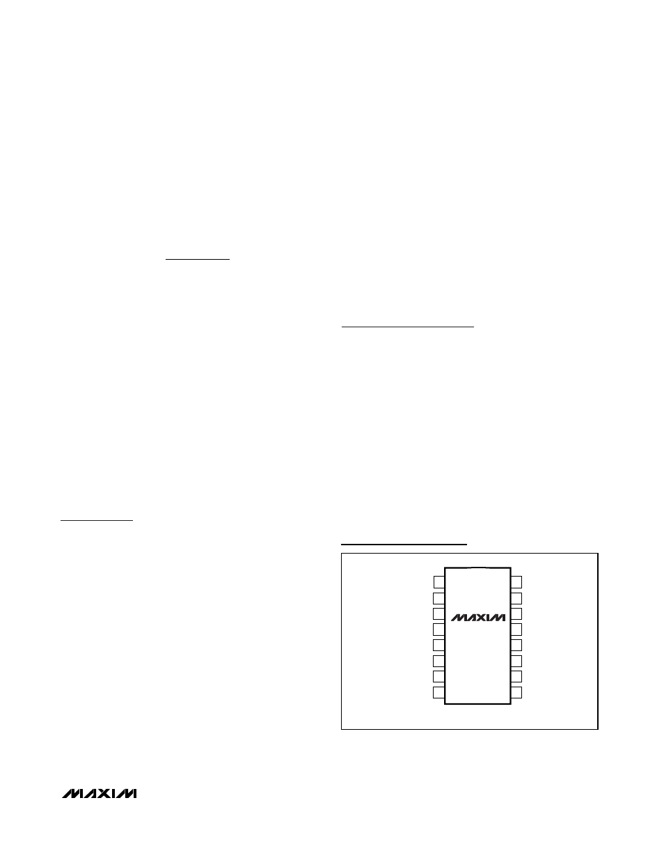
Chip Information
PROCESS: BiCMOS
TRANSISTOR COUNT: 1397
R
R
V
V
ESR
CSB
BATT
REF
<
×
MAX1873
Simple Current-Limited Switch-Mode
Li+ Charger Controller
______________________________________________________________________________________
13
16
15
14
13
12
11
10
9
1
2
3
4
5
6
7
8
CSSN
VL
DCIN
EXT
VH
GND
CSB
BATT
REF
TOP VIEW
MAX1873R/S/T
16 QSOP
CSSP
CCS
ICHG/EN
CCV
CCI
IOUT
VADJ
Pin Configuration
