Step-down dc-dc controllers, Design procedure – Rainbow Electronics MAX652 User Manual
Page 10
__________________Design Procedure
Setting the Output Voltage
The MAX649/MAX651/MAX652 are preset for 5V, 3.3V,
and 3V output voltages, respectively. Tie FB to GND
for fixed-output operation. They may also be adjusted
from 1.5V (the reference voltage) to the input voltage,
using external resistors R2 and R3 configured as
shown in Figure 4. For adjustable-output operation,
150k
Ω
is recommended for resistor R3. 150k
Ω
is a
good value—high enough to avoid wasting energy, yet
low enough to avoid RC delays caused by parasitic
capacitance at FB. R2 is given by:
V
OUT
R2 = R3 x
[
——— -1
]
V
REF
where V
REF
= 1.5V.
When using external resistors, it does no harm to con-
nect OUT and the output together, or to leave OUT
unconnected.
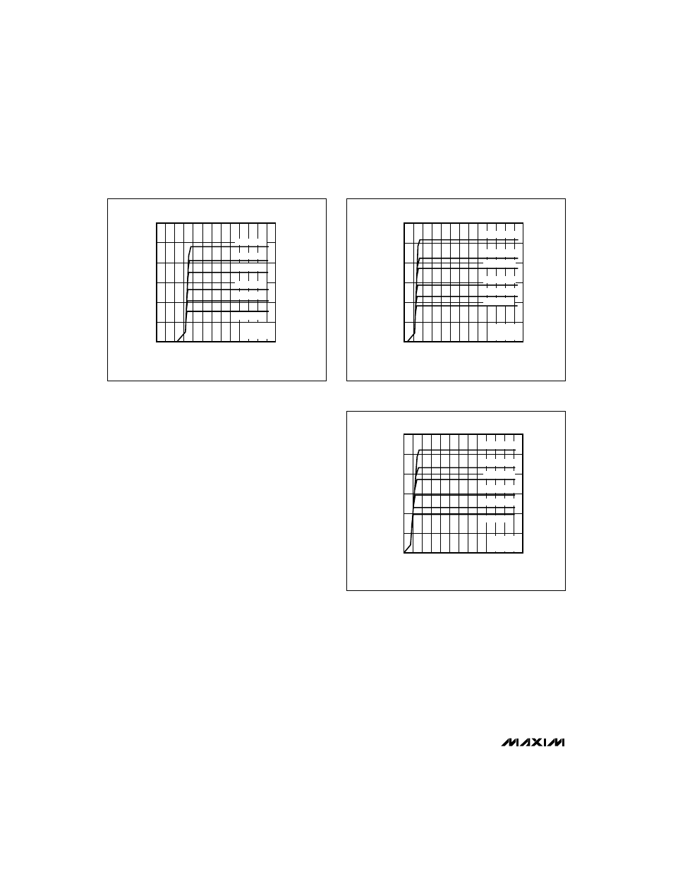
Current-Sense Resistor Selection
The current-sense resistor limits the peak switch cur-
rent to 210mV/R
SENSE
, where R
SENSE
is the value of
the current-sense resistor, and 210mV is the current-
limit trip level (see
Electrical Characteristics).
To maximize efficiency and reduce the size and cost
of external components, minimize the peak current.
However, since the available output current is a func-
tion of the peak current, the peak current must not
be too low.
To choose the proper current-sense resistor for a par-
ticular output voltage, determine the minimum input
voltage and the maximum load current. Next, referring
to Figures 5a, 5b, or 5c, using the minimum input volt-
age, find the curve with the largest sense resistor that
provides sufficient output current. It is not necessary
to perform worst-case calculations. These curves take
into account the worst-case values for sense resistor
(±5%), inductor (22µH ±10%), diode drop (0.6V), and
the IC’s current-sense trip level; an external MOSFET
on-resistance of 0.13
Ω
is assumed for V
GS
= -4.5V.
MAX649/MAX651/MAX652
5V/3.3V/3V or Adjustable, High-Efficiency,
Low I
Q
, Step-Down DC-DC Controllers
10
______________________________________________________________________________________
3.0
0
2.5
MAXIMUM OUTPUT CURRENT (A)
2.0
16
MAX649-A26
INPUT VOLTAGE (V)
14
13
15
0.5
1.0
1.5
12
MAX651
V
OUT
= 3.3V
10
9
11
8
6
5
7
4
3
R
S
= 0.06
Ω
R
S
= 0.07
Ω
R
S
= 0.08
Ω
R
S
= 0.10
Ω
R
S
= 0.12
Ω
R
S
= 0.14
Ω
Figure 5b. MAX651 Current-Sense Resistor Graph
3.0
0
2.5
MAXIMUM OUTPUT CURRENT (A)
2.0
16
MAX649-A27
INPUT VOLTAGE (V)
14
13
15
0.5
1.0
1.5
12
MAX652
V
OUT
= 3.0V
10
9
11
8
6
5
7
4
3
R
S
= 0.06
Ω
R
S
= 0.07
Ω
R
S
= 0.08
Ω
R
S
= 0.10
Ω
R
S
= 0.12
Ω
R
S
= 0.14
Ω
Figure 5c. MAX652 Current-Sense Resistor Graph
3.0
0
2.0
2.5
MAXIMUM OUTPUT CURRENT (A)
9
16
MAX649-A25
INPUT VOLTAGE (V)
7
12
10 11
8
13
0.5
1.0
1.5
6
15
14
4
5
3
MAX649
V
OUT
= 5V
R
S
= 0.06
Ω
R
S
= 0.07
Ω
R
S
= 0.08
Ω
R
S
= 0.10
Ω
R
S
= 0.12
Ω
R
S
= 0.14
Ω
Figure 5a. MAX649 Current-Sense Resistor Graph