Channel slim dsc power supplies, Chip information – Rainbow Electronics MAX1585 User Manual
Page 28
MAX1584/MAX1585
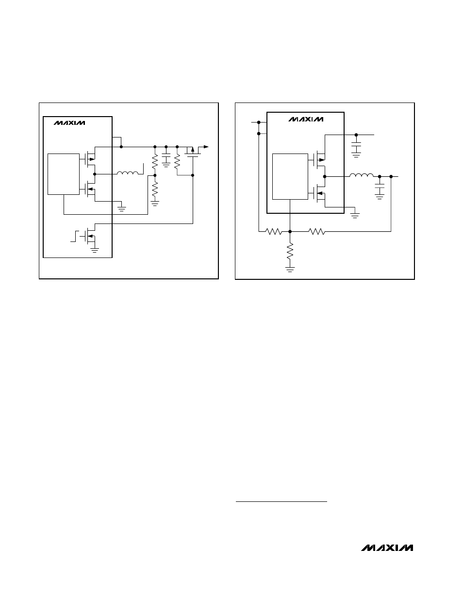
event of an overload. Or, it can remove the load until
the supply reaches regulation, effectively allowing full-
load startup. Figure 15 shows such a connection for the
step-up output.
Setting SDOUT Below 1.25V
The step-down feedback voltage is 1.25V. With a stan-
dard two-resistor feedback network, the output voltage
can be set to values between 1.25V and the input volt-
age. If a step-down output voltage less than 1.25V is
desired, it can be set by adding a third feedback resis-
tor from FBSD to a voltage higher than 1.25V (the step-
up output is a convenient voltage for this) as shown in
Figure 16.
The equation governing output voltage in Figure 16’s
circuit is as follows:
0 = [(V
SD
- V
FBSD
) / R1] + [(0 - V
FBSD
) / R2] + [(V
SU
-
V
FBSD
) / R3]
where V
SD
is the output voltage, V
FBSD
is 1.25V, and
V
SU
is the step-up output voltage. Any available volt-
age that is higher than 1.25V can be used as the con-
nection point for R3 in Figure 16, and for the V
SD
term
in the equation. Since there are multiple solutions for
R1, R2, and R3, the above equation cannot be written
in terms of one resistor. The best method for determin-
ing resistor values is to enter the above equation into a
spreadsheet and test estimated resistor values. A good
starting point is with 100k
Ω at R2 and R3.
Designing a PC Board
Good PC board layout is important to achieve optimal
performance from the MAX1584/MAX1585. Poor design
can cause excessive conducted and/or radiated noise.
Conductors carrying discontinuous currents and any
high-current path should be made as short and wide as
possible. A separate low-noise ground plane contain-
ing the reference and signal grounds should connect to
the power-ground plane at only one point to minimize
the effects of power-ground currents. Typically, the
ground planes are best joined right at the IC.
Keep the voltage-feedback network very close to the
IC, preferably within 0.2in (5mm) of the FB_ pin. Nodes
with high dV/dt (switching nodes) should be kept as
small as possible and should be routed away from
high-impedance nodes such as FB_. Refer to the
MAX1584/MAX1585 evaluation kit data sheet for a full
PC board example.
5-Channel Slim DSC Power Supplies
28
______________________________________________________________________________________
CURRENT-MODE
STEP-UP
PWM
PVSU
PV
LXSU
L2
PGSU
MAX1584
MAX1585
(PARTIAL)
FBSD
SCF
OK
PWR-ON
OR FAULT
V
SU
+5V
TO
V
BATT
Figure 15. SCF controls a PFET load switch to disconnect all
5V loads on fault. This also allows full-load startup.
CURRENT-MODE
STEP-DOWN
PVSD
LXSD
4.7
µH
22
µF
10
µF
PGSD
MAX1584
MAX1585
(PARTIAL)
PVSU
PV
R1
56k
Ω
R3
100k
Ω
R2
100k
Ω
FBSD
V
FBSD
1.25V
V
SU
3.3V
V
SD
0.8V
Figure 16. Setting PVSD for Outputs Below 1.25V
Chip Information
TRANSISTOR COUNT: 8234
PROCESS: BiCMOS