Channel slim dsc power supplies – Rainbow Electronics MAX1585 User Manual
Page 18

MAX1584/MAX1585
end of the soft-start interval. If PVSU is dragged below
the input, the overload is supplied by the body diode of
the internal synchronous rectifier or by a Schottky diode
connected from the battery to PVSU. If desired, this
overload current can be interrupted by a P-channel
MOSFET controlled by SCF, as shown in Figure 15.
Reference
The MAX1584/MAX1585 have internal 1.250V refer-
ences. Connect a 0.1µF ceramic bypass capacitor from
REF to GND within 0.2in (5mm) of the REF pin. REF can
source up to 200µA and is enabled when ONSU is high
and PVSU is above 2.5V. The auxiliary controllers and
MAX1801 slave controllers (if connected) each sink up
to 30µA REF current during startup. If the application
requires that REF be loaded beyond 200µA, buffer REF
with a unity-gain amplifier or op amp.
Oscillator
All MAX1584/MAX1585 DC-DC converter channels
employ fixed-frequency PWM operation. The operating
frequency is set by an RC network at the OSC pin. The
range of usable settings is 100kHz to 1MHz. When
MAX1801 slave controllers are added, they operate at
the frequency set by OSC.
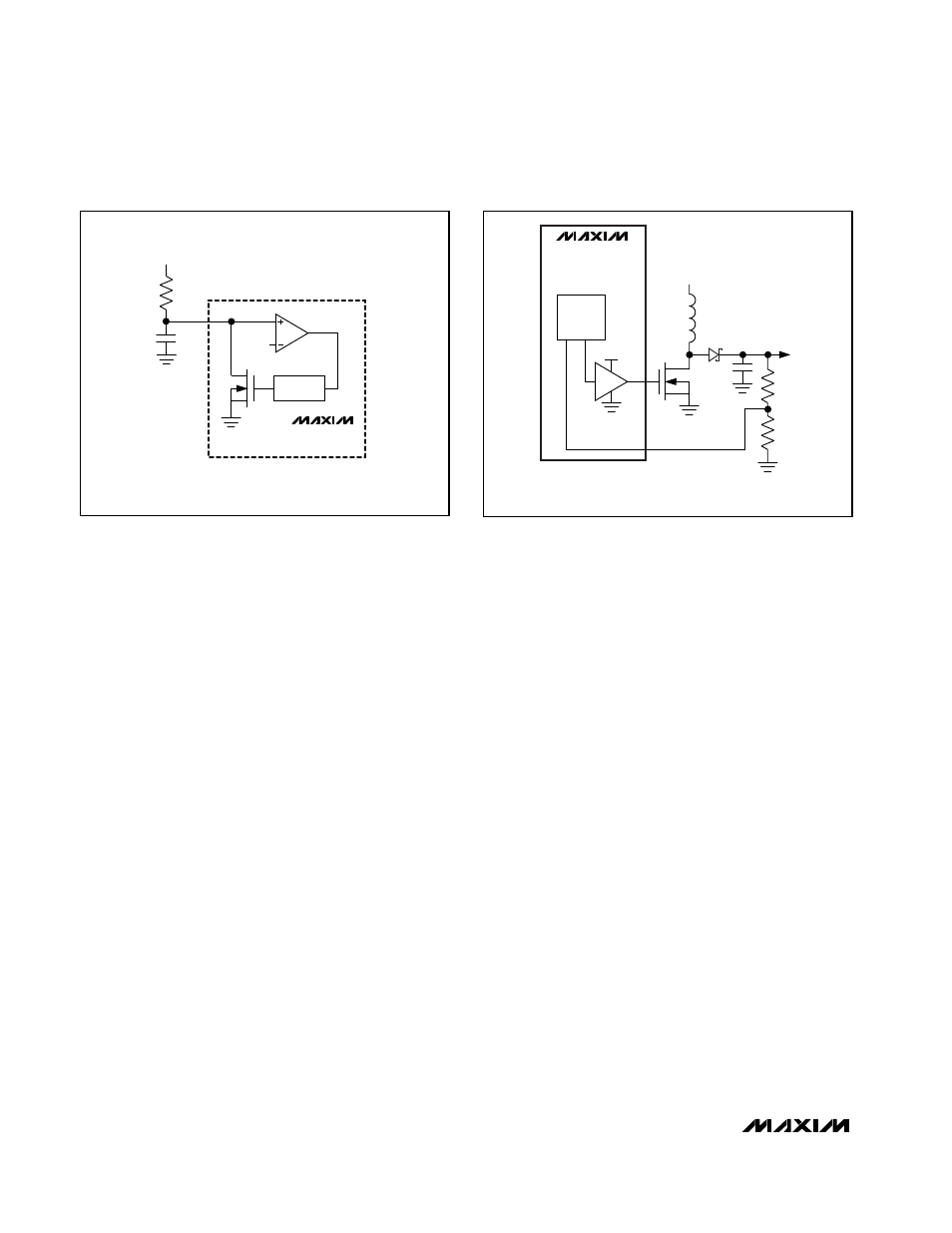
The oscillator uses a comparator, a 150ns one-shot,
and an internal NFET switch in conjunction with an
external timing resistor and capacitor (Figure 4). When
the switch is open, the capacitor voltage exponentially
approaches the step-up output voltage from zero with a
time constant given by the product of R
OSC
and C
OSC
.
The comparator output switches high when the capaci-
tor voltage reaches V
REF
(1.25V). In turn, the one-shot
activates the internal MOSFET switch to discharge the
capacitor within a 150ns interval, and the cycle
repeats. The oscillation frequency changes as the main
output voltage ramps upward following startup. The
oscillation frequency is then constant once the main
output is in regulation.
Low-Voltage Startup Oscillator
The MAX1584/MAX1585 internal control and reference-
voltage circuitry receive power from PVSU and do not
function when PVSU is less than 2.5V. To ensure low-
voltage startup, the step-up employs a low-voltage
startup oscillator that activates at 0.9V if a Schottky rec-
tifier is connected from V
BATT
to PVSU (1.1V with no
Schottky rectifier). The startup oscillator drives the inter-
nal N-channel MOSFET at LXSU until PVSU reaches
2.5V, at which point voltage control is passed to the
current-mode PWM circuitry.
Once in regulation, the MAX1584/MAX1585 operate
with inputs as low as 0.7V since internal power for the
IC is supplied by PVSU. At low input voltages, the step-
up can have difficulty starting into heavy loads (see the
Minimum Startup Voltage vs. Load Current graph in the
Typical Operating Characteristics section); however,
this can be remedied by connecting an external P-
channel load switch driven by SCF so the load is not
connected until the PVSU is in regulation (Figure 15).
ON_ Control Inputs
The step-up converter activates with a high input at
ONSU. The step-down and auxiliary DC-DC converters
1, 2, and 3 activate with a high input at ONSD, ON1,
ON2, and ON3, respectively. The step-down and auxil-
5-Channel Slim DSC Power Supplies
18
______________________________________________________________________________________
C
OSC
V
REF
(1.25V)
V
SU
R
OSC
OSC
150ns
ONE-SHOT
MAX1584
MAX1585
Figure 4. Oscillator Functional Diagram
DL_
FB_
PVSU
AUX
PWM
+15V
50mA
LCD
D6
Q1
TO
V
BATT
MAX1584
MAX1585
(PARTIAL)
NOTE: THIS CIRCUIT CAN OPERATE WITH AUX1 OR
AUX2 ON THE MAX1584, AND WITH AUX1 ON THE MAX1585
Figure 5. +15V LCD Bias with Basic Boost Topology
