Max1729 – Rainbow Electronics MAX1729 User Manual
Page 8
MAX1729
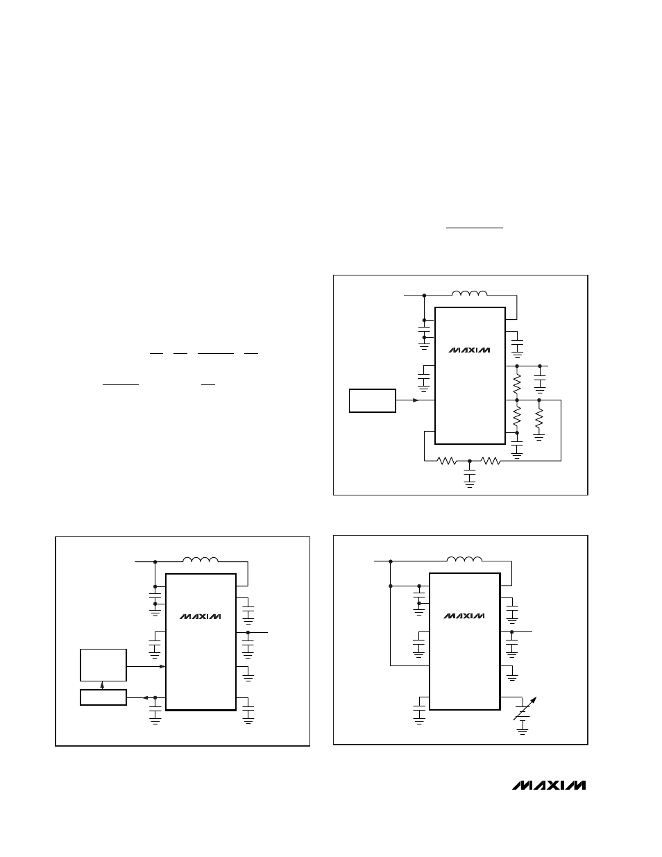
To use a DC control signal to adjust the output voltage,
use the circuit shown in Figure 4. In this configuration,
V
OUT
is governed by the following equation:
The impedance looking into COMP is nominally 33k
Ω
.
A source output impedance of less than 500
Ω
is rec-
ommended. Also, ensure V
OUT
≤
18V by keeping
V
COMP
above 0.6V.
Designing for External Feedback Mode
To solve for V
OUT
in external feedback mode, assume
the current into the FB pin is zero and the voltage at FB
is 1.228V. Then take the sum of the currents into FB
and solve for V
OUT
:
Using the following formulas, calculate the external
component values required for MAX1729 operation in
external feedback mode, as shown in Figure 3. An
example follows the formulas.
External Component Value Formulas
1) Given the maximum output voltage needed (V
MAX
),
choose the maximum feedback current and solve for
R1 (10µA to 30µA is recommended for maximum feed-
back current) as follows:
R1 =
V
- V
I
MAX
FB
FB
V
= R1
1
R1
1
R2
1
R
R
1
R5
V
R1
R
R
V
R1
R5
V
OUT
FB
COMP
TC
+
+
+
+
−
+
−
3
4
3
4
V
24.67V - 22.71V
OUT
FB
COMP
≈
ECB and LCD Display Bias Supply with Accurate
Output Voltage and Temperature Compensation
8
_______________________________________________________________________________________
PS
OUT
FB
COMP
LX
L1
220
µ
H
TC
CTLIN
DIGITAL
PWM
CONTROLLER
GND
IN
V
IN
C1
0.1
µ
F
C2
0.068
µ
F
C4
1
µ
F
C6
1
µ
F
C3
0.1
µ
F
C5
1000pF
V
OUT
MAX1729
REF
ADC
Figure 2. Internal Feedback Mode
PS
OUT
FB
TC
LX
L1
220
µ
H
COMP
CTLIN
PWM
GENERATOR
GND
IN
V
IN
R4
R3
C1
0.1
µ
F
C2
0.068
µ
F
C4
1
µ
F
R1
R5
R2
C6
1
µ
F
C3
0.1
µ
F
V
OUT
MAX1729
C5
1000pF
REF
Figure 3. External Feedback Mode
PS
OUT
FB
COMP
LX
L1
TC
CTLIN
GND
IN
220
µ
H
V
IN
C1
0.1
µ
F
C2
0.068
µ
F
C4
1
µ
F
V
COMP
DC CONTROL
INPUT
C3
0.1
µ
F
C5
1000pF
V
OUT
MAX1729
REF
Figure 4. Using a DC Control Signal