Design procedure – Rainbow Electronics MAX1729 User Manual
Page 7
inductor current to ramp down and V
PS
to increase. If, at
the end of t
OFF
, V
PS
- V
OUT
is still too low, then another
t
ON
is initiated immediately. Otherwise, the boost con-
verter remains idle in a low-quiescent-current state until
V
PS
- V
OUT
drops again and the error comparator initi-
ates another cycle.
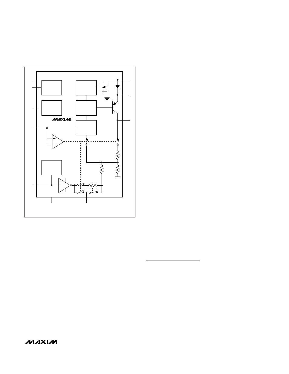
Linear Regulator
The PNP low-dropout linear regulator of the MAX1729
regulates the boost-converter output to the desired out-
put voltage. The boost converter’s regulation circuitry
holds the linear regulator’s input voltage (V
PS
) approxi-
mately 0.6V above the output voltage to keep the regu-
lator out of dropout, thereby enhancing ripple rejection.
The linear regulator incorporates short-circuit protec-
tion, which limits the output current to approximately
6mA.
Temperature Sensor Output
The MAX1729 generates a temperature sensor voltage
(V
TC
) that varies at 16.5mV/°C (typ) and is nominally
equal to the reference voltage at room temperature. TC
is capable of sinking or sourcing 50µA. This output is
used to compensate for ECB color or LCD contrast
variations caused by changes in temperature. It may
be read with an ADC and used to modify an external
PWM control signal or, in external feedback mode,
summed directly into the feedback-resistor network.
Control Signal
An externally generated PWM control signal on CTLIN
controls V
OUT
in internal feedback mode and influ-
ences V
OUT
in external feedback mode. In either mode,
if CTLIN is held low for longer than 1.24ms, the
MAX1729 enters shutdown mode, decreasing the sup-
ply current below 2µA. Shutdown mode limits the mini-
mum duty cycle and frequency that may be used to
keep the device active. CTLIN frequencies between
2kHz and 12kHz are recommended.
Internal Feedback Mode
In internal feedback mode, the signal at CTLIN is inverse-
ly buffered, level-shifted, and output at COMP through a
resistor. Internal resistance (33k
Ω
typical) and C6 then fil-
ter the signal before it is used by the internal feedback
network to set V
OUT
. If temperature compensation is
used, the temperature sensor output voltage is read by
an ADC and used to adjust the duty cycle of the PWM
control signal. See the
Designing for Internal Feedback
Mode
section for more information.
External Feedback Mode
In external feedback mode, the output voltage of the
MAX1729 is controlled by the duty cycle of the PWM
control signal and an external resistor network, as
shown in Figure 3. In this mode, the signal at CTLIN is
inverted, level-shifted, and presented directly to COMP.
R3, R4, and C6 filter the signal, before it is summed into
the feedback node.
Design Procedure
Designing for Internal Feedback Mode
For a 3kHz PWM control signal use a 1µF low-leakage
ceramic capacitor for C6. For applications requiring a
higher-frequency PWM control signal, reduce the value
of C6 to between 1µF and 0.22µF for frequencies
between 3kHz and 12kHz. Higher C6 values reduce
output ripple. In Figure 2, V
OUT
is governed by the fol-
lowing equation:
where V
OUT(MIN)
is 2.45V and Gain is nominally
13.95V/100%, as listed in the
Electrical Characteristics.
V
= V
Duty Cycle Gain
OUT
OUT(MIN)
+
⋅
MAX1729
ECB and LCD Display Bias Supply with Accurate
Output Voltage and Temperature Compensation
_______________________________________________________________________________________
7
122mV
V
REF
GND
NOTE: SWITCH STATES SHOWN FOR INTERNAL FEEDBACK MODE.
COMP
TC
LX
PS
OUT
MAX1729
IN
REF
FB
CTLIN
BOOST
CONVERTER
TEMPERATURE
SENSOR
VOLTAGE
REFERENCE
SHUTDOWN
CONTROL
LDO
LINEAR
REGULATOR
FEEDBACK
CONTROL
GND
Figure 1. Internal Block Diagram