Rainbow Electronics MAX1729 User Manual
Page 2
MAX1729
ECB and LCD Display Bias Supply with Accurate
Output Voltage and Temperature Compensation
2
_______________________________________________________________________________________
ABSOLUTE MAXIMUM RATINGS
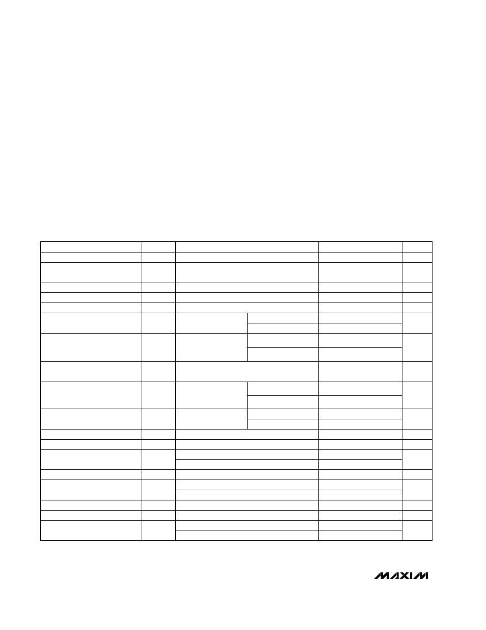
ELECTRICAL CHARACTERISTICS
(V
IN
= +3V, CTLIN = IN, FB = GND, T
A
= -40°C to +85°C, unless otherwise noted. Typical values are at T
A
= +25°C.) (Note 1)
Stresses beyond those listed under “Absolute Maximum Ratings” may cause permanent damage to the device. These are stress ratings only, and functional
operation of the device at these or any other conditions beyond those indicated in the operational sections of the specifications is not implied. Exposure to
absolute maximum rating conditions for extended periods may affect device reliability.
IN to GND .................................................................-0.3V to +6V
LX, PS, OUT to GND...............................................-0.3V to +20V
CTLIN, FB, REF, COMP, TC to GND ...........-0.3V to (V
IN
+ 0.3V)
LX to PS ..................................................................-20V to +1.0V
LX, PS, OUT Current ...........................................................60mA
Continuous Power Dissipation (T
A
= +70°C)
10-pin µMAX (derate 5.6mW/°C above +70°C) ..........444mW
Operating Temperature Range ...........................-40°C to +85°C
Junction Temperature ......................................................+150°C
Storage Temperature Range .............................-65°C to +160°C
Lead Temperature (soldering, 10sec) .............................+300°C
CONDITIONS
V
2.7
5.5
V
IN
Operating Voltage Range
UNITS
MIN
TYP
MAX
SYMBOL
PARAMETER
V
2.0
2.6
V
LO
Undervoltage Lockout
Threshold (Note 2)
µA
37
50
I
IN
IN Supply Current
µA
30
40
I
PS
PS Supply Current
µA
0.4
2
I
SHDN
Shutdown Supply Current
CTLIN = GND, I
SHDN
= I
IN
+ I
PS
I
REF
= 0
V
1.215
1.228
1.241
V
REF
Reference Output Voltage
T
A
= +25°C
1.200
1.256
T
A
= -40°C to +85°C
FB = GND, CTLIN =
0.1% duty cycle,
I
OUT
= 0 to 0.5mA
V
V
OUT
(MIN)
Minimum Output Voltage
2.35
2.45
2.5
T
A
= -40°C to +85°C
I
OUT
= 0 to 0.5mA
V
16
16.40
V
OUT
(MAX)
Maximum Output Voltage
FB = GND, CTLIN =
0.1% to 100% duty
cycle, I
OUT
= 0
V/100%
CTLIN to V
OUT
Gain
13.90
13.95
14.00
T
A
= 0°C to +85°C
V
PS
= +18V (Note 3)
ppm/°C
±11
±30
TC
OUT
Output Voltage
Temperature Coefficient
T
A
= 0°C to +85°C
±18
±65
T
A
= -40°C to +85°C
mA
0.5
2.5
I
OUT
Maximum Output Current
V
1.178
1.228
1.278
V
TC
TC Output Voltage
T
A
= +25°C
mV/°C
15.5
16.5
17.5
TC
TC
TC Output Temperature
Coefficient (Note 3)
T
A
= 0°C to +85°C
14.5
16.5
18.5
T
A
= -40°C to +85°C
µA
±50
I
TC
TC Output Current
T
A
= 0°C to +85°C
2.35
2.52
T
A
= -40°C to +85°C
13.60
14.20
V
1.215
1.228
1.241
V
FB
Feedback Set Voltage (FB)
T
A
= +25°C
1.200
1.256
T
A
= -40°C to +85°C
mV
90
122
150
V
MODE
FB Mode Threshold
nA
5
50
I
FB
FB Bias Current
V
FB
= +1.25V
V
2
V
IH
CTLIN High Voltage
V
IN
= +5.5V
1.3
V
IN
= +2.7V