Chip information, Paralleling devices, Combined doubler/inverter – Rainbow Electronics MAX1721 User Manual
Page 8: Heavy load connected to a positive supply, Layout and grounding
MAX1719/MAX1720/MAX1721
SOT23, Switched-Capacitor
Voltage Inverters with Shutdown
Maxim cannot assume responsibility for use of any circuitry other than circuitry entirely embodied in a Maxim product. No circuit patent licenses are
implied. Maxim reserves the right to change the circuitry and specifications without notice at any time.
8
_____________________Maxim Integrated Products, 120 San Gabriel Drive, Sunnyvale, CA 94086 408-737-7600
© 1999 Maxim Integrated Products
Printed USA
is a registered trademark of Maxim Integrated Products.
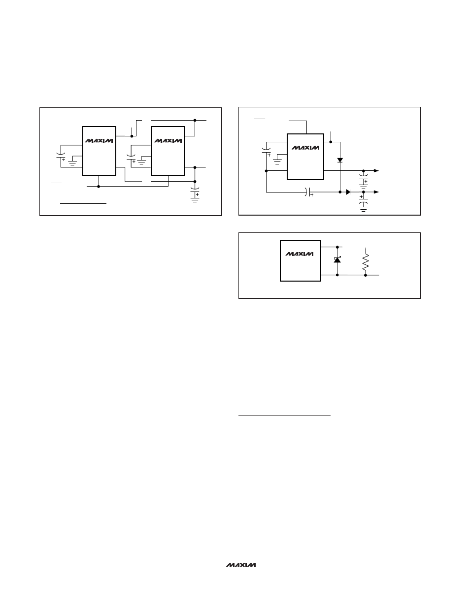
Paralleling Devices
Paralleling multiple MAX1719s, MAX1720s, or
MAX1721s reduces the output resistance. Each device
requires its own pump capacitor (C1), but the reservoir
capacitor (C2) serves all devices (Figure 5). Increase
C2’s value by a factor of n, where n is the number of
parallel devices. Figure 5 shows the equation for calcu-
lating output resistance.
Combined Doubler/Inverter
In the circuit of Figure 6, capacitors C1 and C2 form the
inverter, while C3 and C4 form the doubler. C1 and C3
are the pump capacitors; C2 and C4 are the reservoir
capacitors. Because both the inverter and doubler use
part of the charge-pump circuit, loading either output
causes both outputs to decline toward GND. Make sure
the sum of the currents drawn from the two outputs
does not exceed 25mA.
Heavy Load Connected to a
Positive Supply
Under heavy loads, where a higher supply is sourcing
current into OUT, the OUT supply must not be pulled
above ground. Applications that sink heavy current into
OUT require a Schottky diode (1N5817) between GND
and OUT, with the anode connected to OUT (Figure 7).
Layout and Grounding
Good layout is important, primarily for good noise per-
formance. To ensure good layout, mount all compo-
nents as close together as possible, keep traces short
to minimize parasitic inductance and capacitance, and
use a ground plane.
MAX1719
MAX1720
MAX1721
2
5
1
V
OUT
= (2V
IN
) -
(V
FD1
) - (V
FD2
)
C2
+V
IN
C1
3
4
6
V
OUT
= -V
IN
C4
D1
D1, D2 = 1N4148
C3
D2
SHDN (MAX1719)
SHDN (MAX1720/
MAX1721)
Figure 6. Combined Doubler and Inverter
MAX1719
MAX1720
MAX1721
4
1
GND
OUT
V+
R
L
Figure 7. Heavy Load Connected to a Positive Supply
TRANSISTOR COUNT: 85
MAX1719
MAX1720
MAX1721
“n”
MAX1719
MAX1720
MAX1721
“1”
2
1
V
OUT
C2
2
+V
IN
C1
C1
3
3
4
4
6
5
5
6
1
V
OUT
= -V
IN
R
O
=
R
O
OF SINGLE DEVICE
NUMBER OF DEVICES
…
…
SHDN (MAX1719)
SHDN (MAX1720/
MAX1721)
Figure 5. Paralleling MAX1719s or MAX1720s or MAX1721s to
Reduce Output Resistance
Chip Information