Applications information – Rainbow Electronics MAX1721 User Manual
Page 7
MAX1719/MAX1720/MAX1721
SOT23, Switched-Capacitor
Voltage Inverters with Shutdown
_______________________________________________________________________________________
7
Surface-Mount
Tantalum
PRODUCTION
METHOD
714-969-2491
803-946-0690
PHONE
603-224-1961
603-224-1430
714-960-6492
803-626-3123
FAX
MANUFACTURER
AVX
Matsuo
Sprague
SERIES
TPS series
267 series
593D, 595D series
714-969-2491
803-946-0690
AVX
Matsuo
714-960-6492
803-626-3123
X7R
X7R
Surface-Mount
Ceramic
Table 2. Capacitor Selection for Minimum Output Resistance or Capacitor Size
Table 1. Low-ESR Capacitor Manufacturers
f
OSC
CAPACITORS TO MINIMIZE SIZE
(R
O
= 40
Ω
, TYP)
C1 = C2
0.33µF
3.3µF
12kHz
CAPACITORS TO MINIMIZE
OUTPUT RESISTANCE
(R
O
= 23
Ω
, TYP)
C1 = C2
125kHz
10µF
1µF
MAX1720
PART
MAX1719/MAX1721
Applications Information
Capacitor Selection
To maintain the lowest output resistance, use capaci-
tors with low ESR (Table 1). The charge-pump output
resistance is a function of C1’s and C2’s ESR.
Therefore, minimizing the charge-pump capacitor’s
ESR minimizes the total output resistance. Table 2
gives suggested capacitor values for minimizing output
resistance or minimizing capacitor size.
Flying Capacitor (C1)
Increasing the flying capacitor’s value reduces the out-
put resistance. Above a certain point, increasing C1’s
capacitance has a negligible effect because the output
resistance becomes dominated by the internal switch
resistance and capacitor ESR.
Output Capacitor (C2)
Increasing the output capacitor’s value reduces the
output ripple voltage. Decreasing its ESR reduces both
output resistance and ripple. Lower capacitance values
can be used with light loads if higher output ripple can
be tolerated. Use the following equation to calculate the
peak-to-peak ripple:
Input Bypass Capacitor (C3)
Bypass the incoming supply to reduce its AC impedance
and the impact of the MAX1719/MAX1720/MAX1721’s
switching noise. A bypass capacitor with a value equal
to that of C1 is recommended.
Voltage Inverter
The most common application for these devices is a
charge-pump voltage inverter (Figure 1). This applica-
tion requires only two external components—capacitors
C1 and C2—plus a bypass capacitor, if necessary.
Refer to the
Capacitor Selection
section for suggested
capacitor types.
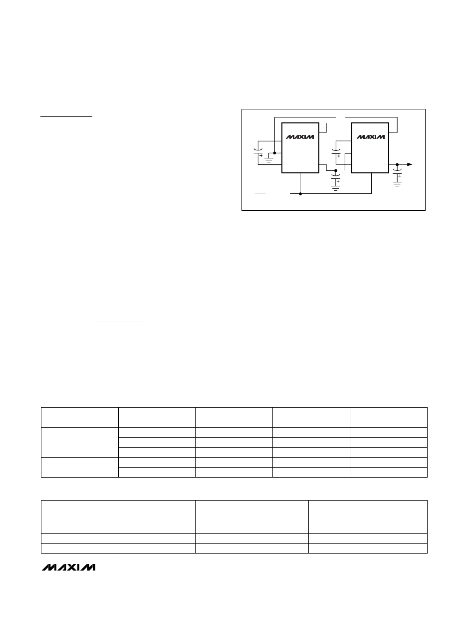
Cascading Devices
Two devices can be cascaded to produce an even
larger negative voltage (Figure 4). The unloaded output
voltage is normally -2
·
V
IN
, but this is reduced slightly
by the output resistance of the first device multiplied by
the quiescent current of the second. When cascading
more than two devices, the output resistance rises dra-
matically. For applications requiring larger negative
voltages, see the MAX865 and MAX868 data sheets.
V
=
I
2 x f
C2
2 I
ESR
RIPPLE
OUT
OSC
OUT
C2
⋅
⋅
⋅
+
MAX1719
MAX1720
MAX1721
“n”
MAX1719
MAX1720
MAX1721
“1”
2
1
V
OUT
C2
2
+V
IN
C1
C2
SHDN (MAX1719)
SHDN (MAX1720/
MAX1721)
C1
3
3
4
4
6
5
5
6
1
V
OUT
= -nV
IN
…
…
Figure 4. Cascading MAX1719s or MAX1720s or MAX1721s
to Increase Output Voltage