Chip information – Rainbow Electronics MAX1683 User Manual
Page 7

Cascading Devices
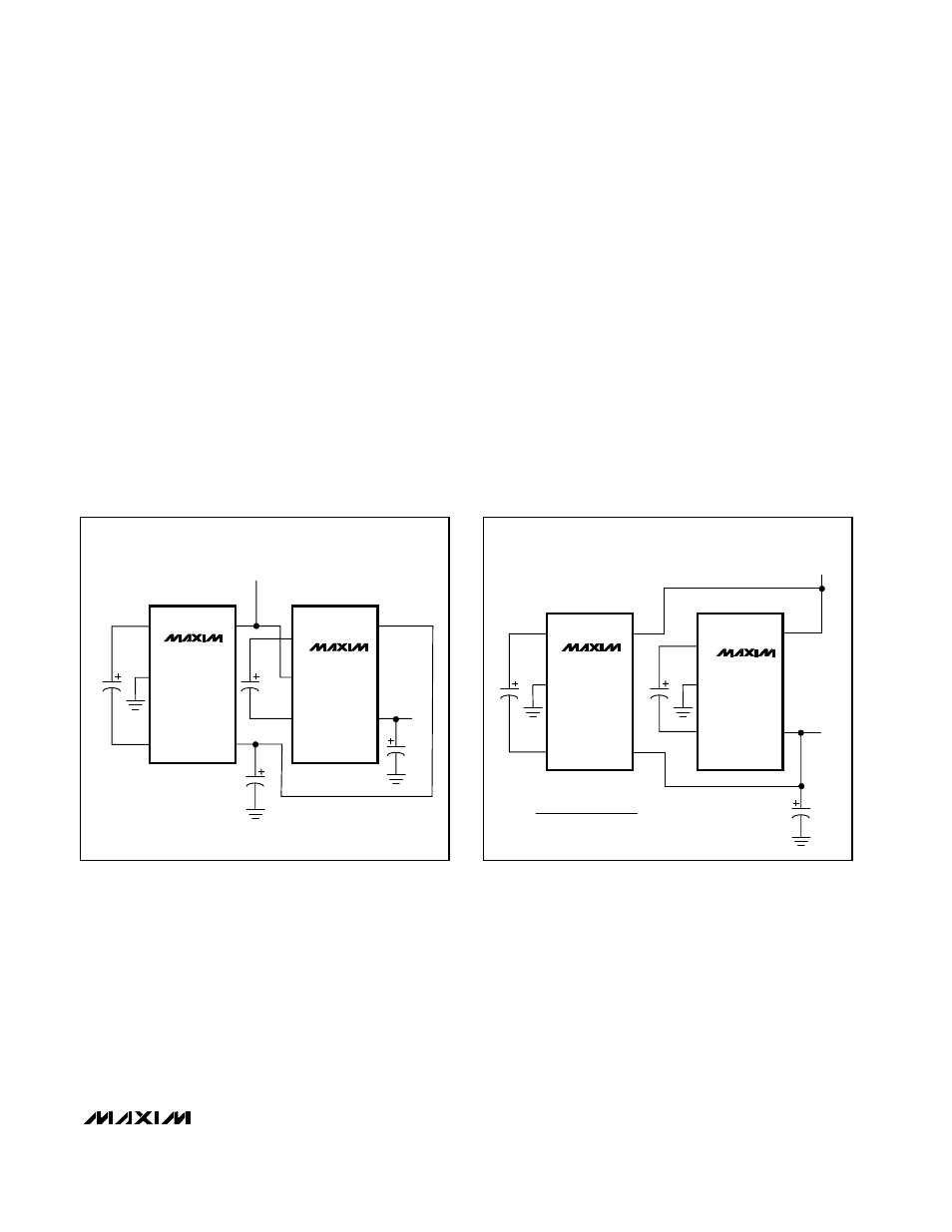
Devices can be cascaded to produce an even larger
voltage (Figure 3). The unloaded output voltage is nom-
inally (n + 1) x V
IN
, where n is the number of voltage
doublers used. This voltage is reduced by the output
resistance of the first device multiplied by the quiescent
current of the second. The output resistance increases
when devices are cascaded. Using a two-stage dou-
bler as an example, output resistance can be approxi-
mated as R
OUT
= 2 x R
OUT1
+ R
OUT2
, where R
OUT1
is
the output resistance of the first stage and R
OUT2
is the
output resistance of the second stage. A typical value
for a two-stage voltage doubler is 60
Ω (with C1 at 10µF
for MAX1682 and 3.3µF for MAX1683). For n stages
with the same C1 value, R
OUT
= (2
n
- 1) x R
OUT1
.
Paralleling Devices
Paralleling multiple MAX1682 or MAX1683s reduces
the output resistance. Each device requires its own
pump capacitor (C1), but the reservoir capacitor (C2)
serves all devices (Figure 4). Increase C2’s value by a
factor of n, where n is the number of parallel devices.
Figure 4 shows the equation for calculating output
resistance.
Layout and Grounding
Good layout is important, primarily for good noise per-
formance. To ensure good layout, mount all compo-
nents as close together as possible, keep traces short
to minimize parasitic inductance and capacitance, and
use a ground plane.
MAX1682/MAX1683
Switched-Capacitor Voltage Doublers
_______________________________________________________________________________________
7
MAX1682
MAX1683
C1
C2
C2
C1+
IN
OUT
GND
C1-
MAX1682
MAX1683
C1
C1+
INPUT
SUPPLY
VOLTAGE
OUTPUT
VOLTAGE
IN
OUT
GND
C1-
Figure 3. Cascading Devices
MAX1682
MAX1683
R
OUT
=
R
OUT
OF SINGLE DEVICE
NUMBER OF DEVICES
C2
C1+
IN
OUT
GND
C1-
MAX1682
MAX1683
C1
C1
C1+
INPUT
SUPPLY
VOLTAGE
OUTPUT
VOLTAGE
IN
OUT
GND
C1-
Figure 4. Paralleling Devices
___________________Chip Information
TRANSISTOR COUNT: 97
