Switched-capacitor voltage doublers, Applications information – Rainbow Electronics MAX1683 User Manual
Page 6
MAX1682/MAX1683
Conversion losses occur during the charge transfer
between C1 and C2 when there is a voltage difference
between them. The power loss is:
where V
RIPPLE
is the peak-to-peak output voltage ripple
determined by the output capacitor and load current
(see Output Capacitor section). Choose capacitor val-
ues that decrease the output resistance (see Flying
Capacitor section).
Applications Information
Flying Capacitor (C1)
To maintain the lowest output resistance, use capaci-
tors with low ESR. Suitable capacitor manufacturers are
listed in Table 1. The charge-pump output resistance is
a function of C1 and C2’s ESR and the internal switch
resistance, as shown in the equation for R
OUT
in the
Efficiency Considerations section.
Minimizing the charge-pump capacitor’s ESR mini-
mizes the total resistance. Suggested values are listed
in Tables 2 and 3.
Using a larger flying capacitor reduces the output
impedance and improves efficiency (see the Efficiency
Considerations section). Above a certain point, increas-
ing C1’s capacitance has a negligible effect because
the output resistance becomes dominated by the inter-
nal switch resistance and capacitor ESR (see the
Output Resistance vs. Capacitance graph in the
Typical Operating Characteristics). Table 2 lists the
most desirable capacitor values—those that produce a
low output resistance. But when space is a constraint, it
may be necessary to sacrifice low output resistance for
the sake of small capacitor size. Table 3 demonstrates
how the capacitor affects output resistance.
Output Capacitor (C2)
Increasing the output capacitance reduces the output
ripple voltage. Decreasing its ESR reduces both output
resistance and ripple. Smaller capacitance values can
be used with light loads. Use the following equation to
calculate the peak-to-peak ripple:
V
RIPPLE
= I
OUT
/ (f
OSC
x C2) + 2 x I
OUT
x ESR
C2
Input Bypass Capacitor
Bypass the incoming supply to reduce its AC imped-
ance and the impact of the MAX1682/MAX1683’s
switching noise. When loaded, the circuit draws a con-
tinuous current of 2 x I
OUT
. A 0.1µF bypass capacitor is
sufficient.
P
/ C1 4V
V
/ C2 2V
V
V
x f
CONVERSION LOSS
1 2
IN
2
OUT
2
1 2
OUT RIPPLE
2
RIPPLE
OSC
=
−
+
−
Switched-Capacitor Voltage Doublers
6
_______________________________________________________________________________________
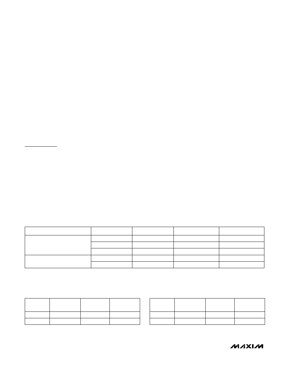
Table 1. Recommended Capacitor Manufacturers
Table 2. Suggested Capacitor Values for
Low Output Resistance
Table 3. Suggested Capacitor Values for
Minimum Size
MANUFACTURER
AVX
PRODUCTION METHOD
SERIES
TPS
PHONE
FAX
803-946-0690
803-448-2170
Matsuo
267
714-969-2491
714-960-6492
Surface-Mount Tantalum
Sprague
593D, 595D
603-224-1961
603-224-1430
AVX
X7R
803-946-0590
803-626-3123
Surface-Mount Ceramic
Matsuo
X7R
714-969-2491
714-960-6492
PART
FREQUENCY
(kHz)
MAX1682
12
MAX1683
35
CAPACITOR
VALUE (µF)
10
3.3
TYPICAL
R
OUT
(
Ω)
20
20
PART
FREQUENCY
(kHz)
CAPACITOR
VALUE (µF)
MAX1682
12
3.3
1
TYPICAL
R
OUT
(
Ω)
35
35
MAX1683
35