Detailed description, Pin description – Rainbow Electronics MAX1683 User Manual
Page 5
_______________Detailed Description
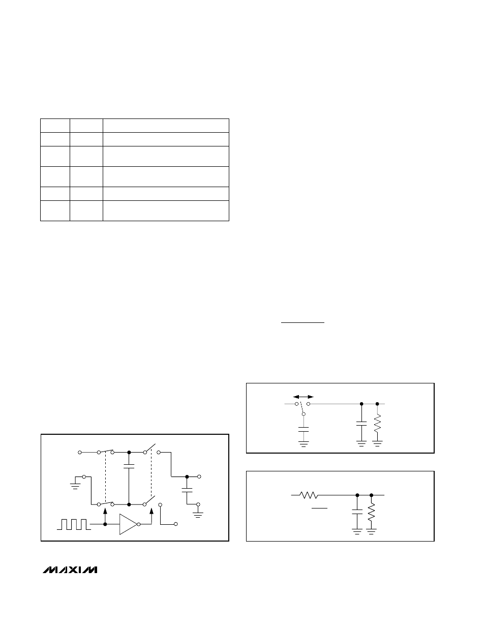
The MAX1682/MAX1683 capacitive charge pumps
double the voltage applied to their input. Figure 1
shows a simplified functional diagram of an ideal volt-
age doubler. During the first half-cycle, switches S1
and S2 close, and capacitor C1 charges to V
IN
. During
the second half cycle, S1 and S2 open, S3 and S4
close, and C1 is level shifted upward by V
IN
volts. This
connects C1 to the reservoir capacitor C2, allowing
energy to be delivered to the output as necessary. The
actual voltage is slightly lower than 2 x V
IN
, since
switches S1–S4 have resistance and the load drains
charge from C2.
Charge-Pump Output
The MAX1682/MAX1683 have a finite output resistance
of about 20
Ω (Table 2). As the load current increases,
the devices’ output voltage (V
OUT
) droops. The droop
equals the current drawn from V
OUT
times the circuit’s
output impedance (R
S
), as follows:
V
DROOP
= I
OUT
x R
S
V
OUT
= 2 x V
IN
- V
DROOP
Efficiency Considerations
The power efficiency of a switched-capacitor voltage
converter is affected by three factors: the internal losses
in the converter IC, the resistive losses of the capacitors,
and the conversion losses during charge transfer
between the capacitors. The total power loss is:
The internal losses are associated with the IC’s internal
functions, such as driving the switches, oscillator, etc.
These losses are affected by operating conditions such
as input voltage, temperature, and frequency.
The next two losses are associated with the voltage
converter circuit’s output resistance. Switch losses
occur because of the on-resistance of the MOSFET
switches in the IC. Charge-pump capacitor losses
occur because of their ESR. The relationship between
these losses and the output resistance is as follows:
where f
OSC
is the oscillator frequency. The first term is
the effective resistance from an ideal switched-
capacitor circuit (Figures 2a and 2b).
P
P
I
x R
R
f
x C
R
ESR
ESR
PUMP CAPACITOR LOSSES
SWITCH LOSSES
OUT
OUT
OUT
OSC
SWITCHES
C
C
+
=
≅
(
)
+
+
+
2
1
2
1
1
2
4
ΣP
P
P
P
LOSS
INTERNAL LOSSES
PUMP CAPACITOR LOSSES
CONVERSION LOSSES
=
+
+
MAX1682/MAX1683
Switched-Capacitor Voltage Doublers
_______________________________________________________________________________________
5
_____________________Pin Description
NAME
FUNCTION
1
GND
Ground
2
OUT
Doubled Output Voltage. Connect C2
between OUT and GND.
PIN
3
C1-
Negative Terminal of the Flying
Capacitor
4
IN
Input Supply
5
C1+
Positive Terminal of the Flying
Capacitor
Figure 2a. Switched-Capacitor Model
V+
C1
f
C2
R
L
V
OUT
Figure 1. Simplified Functional Diagram of Ideal Voltage
Doubler
S1
V
IN
S3
S2
V
IN
V
OUT
S4
C1
C2
Figure 2b. Equivalent Circuit
R
EQUIV
=
R
EQUIV
V
OUT
R
L
1
V+
f
× C1
C2