Applications information – Rainbow Electronics MAX726 User Manual
Page 9
MAX724/MAX726
5A/2A Step-Down, PWM,
Switch-Mode DC-DC Regulators
_______________________________________________________________________________________
9
Be sure that the selected capacitor can handle the ripple
current over the required temperature range. Also locate
the input capacitor very close to the MAX724/MAX726 and
use minimum length leads (surface-mount or radial
through-hole types). In most applications, ESR is more
important than actual capacitance value since electrolytic
capacitors are mostly resistive at the MAX724/MAX726's
100kHz switching frequency.
__________Applications Information
Setting Output Voltage
R1 and R2 set output voltage as follows:
R1 =
V
OUT
R2
2.21V
-R2
2.21V is the reference voltage, so setting R2 to 2.21k
Ω
(standard 1% resistor value) results in 1mA flowing
through R1 and R2 and simplifies the above equation.
Other values will also work for R2, but should not
exceed 4k
Ω
.
Synchronizing the Oscillator
The MAX724/MAX726 can be synchronized to an exter-
nal 110kHz to 160kHz source by pulsing the V
C
pin to
ground at the desired clock rate. This is conveniently
done with the collector of an external grounded-emitter
NPN transistor. V
C
should be pulled low for 300ns.
Doing this may have some impact on output regulation,
but the effect should be minimal for compensation
resistor values between 1k
Ω
and 4k
Ω
.
Power Dissipation
The MAX724/MAX726 draw about 7.5mA operating cur-
rent, which is largely independent of input voltage or
load current. They draw an additional 5mA during
switch on-time. Power dissipated in the internal V
SW
transistor is proportional to load current and depends
on both conduction losses (product of switch on-volt-
age and switch current) and dynamic switching losses
(due to switch rise and fall times). Total MAX724 power
dissipation can be calculated as follows:
P = V
IN
[7.5mA + 5mA (DC) + 2 I
OUT
t
SW
f
OSC
] + . . .
. . . DC [I
OUT
(1.8V) + 0.1
Ω
(I
OUT
)
2
]
DC = Duty Cycle =
V
OUT
+ 0.5V
V
IN
- 2V
t
SW
= Overlap Time = 50ns + (3ns/A) I
OUT
where t
SW
is "overlap" time. Switch dissipation is
momentarily high during overlap time because both cur-
rent and voltage appear across the switch at the same
time. t
SW
is approximately: [50ns + (3ns/A) (I
OUT
)] for
the MAX724.
Power dissipation in the MAX726 can be estimated in
exactly the same way as the MAX724, except that 1.1V
(and not 1.8V) is a more reasonable value for the nomi-
nal voltage drop across the on-board power switch.
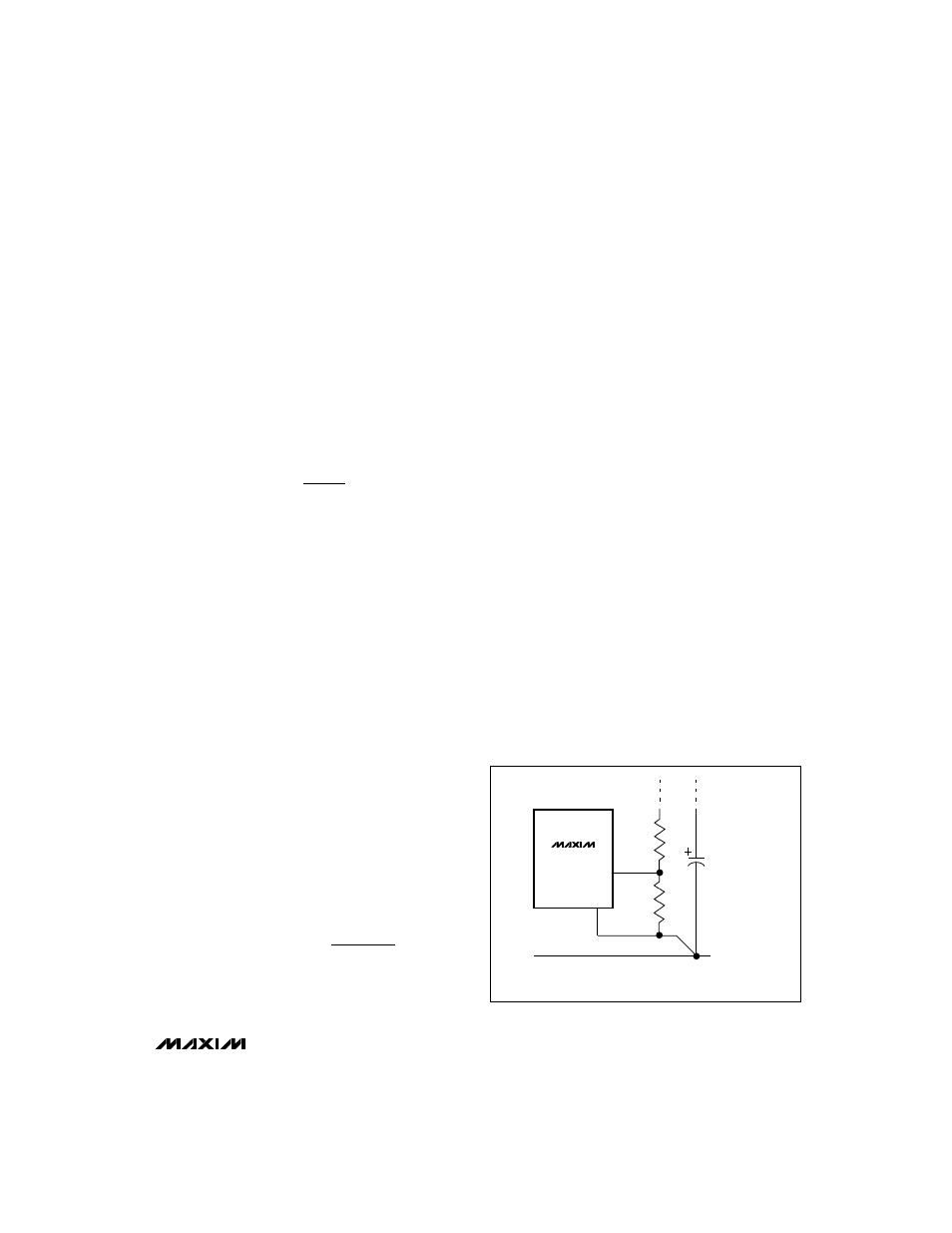
Ground Connections
GND demands a short low-noise connection to ensure
good load regulation. Since the internal reference is
referred to GND, errors in the GND pin voltage get mul-
tiplied by the error amplifier and appear at the output.
If the MAX724/MAX726 GND pin is separated from the
negative side of the load, then high load return current
can generate significant error across a seemingly small
ground resistance. Single-point grounding is the most
effective way to eliminate these errors. A recommend-
ed ground arrangement is shown in Figure 4.
Overload Protection
The V
SW
current is internally limited to about 6.5A in the
MAX724 and 2.6A in the MAX726. In addition, another
feature of the MAX724/MAX726's overload protection
scheme is that the oscillator frequency is reduced
when the output voltage falls below approximately half
its regulated value. This is the case during short-circuit
and heavy overload conditions.
Since the minimum on-time for the switch is about
0.6
µ
s, frequency reduction during overload ensures
that switch duty cycle can fall to a low enough value to
maintain control of output current. At the normal
100kHz switching frequency, an on-time as short as
R1
R2
FB
GND
HIGH CURRENT
RETURN PATH
NEGATIVE OUTPUT
NODE WHERE LOAD
REGULATION WILL
BE MEASURED
MAX724
MAX726
Figure 4. Recommended Ground Connection