Typical operating characteristics, Electrical characteristics (continued) – Rainbow Electronics MAX726 User Manual
Page 3
MAX724/MAX726
5A/2A Step-Down, PWM,
Switch-Mode DC-DC Regulators
_______________________________________________________________________________________
3
ELECTRICAL CHARACTERISTICS (continued)
(V
IN
= 25V, T
j
= T
MIN
to T
MAX
, unless otherwise noted.)
Note 1:
Do not exceed switch-to-input voltage limitation.
Note 2:
For switch currents between 1A and 5A (2A for MAX726), maximum switch-on voltage can be calculated via linear
interpolation.
Note 3:
By setting the feedback pin (FB) to 2.5V, the V
C
pin is forced to its low clamp level and the switch duty cycle is forced to
zero, approximating the zero load condition.
Note 4:
For proper regulation, total voltage from V
IN
to GND must be
≥
8V after start-up.
Note 5:
To avoid extremely short switch-on times, the switch frequency is internally scaled down when V
FB
is less than 1.3V. Switch-
current limit is tested with V
FB
adjusted to give a 1µs minimum switch-on time.
Note 6:
Guaranteed, not production tested.
PARAMETER
CONDITIONS
MIN
TYP
MAX
UNITS
Error-Amplifier Voltage Gain
1V
≤
V
C
≤
4V
T
j
= +25°C
2000
V/V
Error-Amplifier Transconductance
T
j
= +25°C
3000 5000 9000
µmho
Error-Amplifier Source Current
V
FB
= 2V
T
j
= +25°C
100
140
225
µA
Reference Voltage Tolerance
VREF (nominal) = 2.21V
T
j
= +25°C
±0.5
±1.5
%
Reference Voltage
V
C
= 2V
2.155 2.210 2.265
V
Feedback Pin Bias Current
V
FB
= VREF
0.5
2
µA
Error-Amplifier Sink Current
V
FB
= 2.5V
T
j
= +25°C
0.6
1.0
1.7
mA
T
j
= T
MIN
to T
MAX
-4
mV/°C
VC Voltage at 0% Duty Cycle
T
j
= +25°C
1.5
V
Reference Voltage Line Regulation
8V
≤
V
IN
≤
40V
0.005 0.02
%/V
±1.0
±2.5
MAX724
2.5
°C/W
Thermal Resistance,
Junction to Case (Note 6)
All conditions of input voltage, output voltage,
temperature and load current
MAX726
4.0
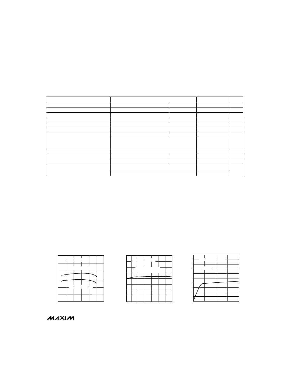
__________________________________________Typical Operating Characteristics
110
50
0
6
MAX724
STEP-DOWN CONVERTER EFFICIENCY
vs. OUTPUT CURRENT
60
100
OUTPUT CURRENT (A)
EFFICIENCY (%)
4
80
70
1
3
5
90
2
CIRCUIT OF FIGURE 2
V
OUT
= 12V, V
IN
= 20V
V
OUT
= 5V, V
IN
= 15V
16
4
-40
100
SUPPLY CURRENT
vs. JUNCTION TEMPERATURE
6
14
JUNCTION TEMPERATURE (°C)
SUPPLY CURRENT (mA)
50
10
8
-25
25
75
12
0
CIRCUIT OF FIGURE 2
V
IN
= 25V, V
OUT
= 5V
I
OUT
= 1mA
2
0
125
20
8
0
QUIESCENT SUPPLY CURRENT
vs. INPUT VOLTAGE
10
18
V
IN
INPUT VOLTAGE (V)
QUIESCENT SUPPLY CURRENT (mA)
40
14
12
10
30
16
20
6
4
V
C
= 1V
DEVICE NOT SWITCHING
2
0