Typical applications – Rainbow Electronics MAX726 User Manual
Page 11
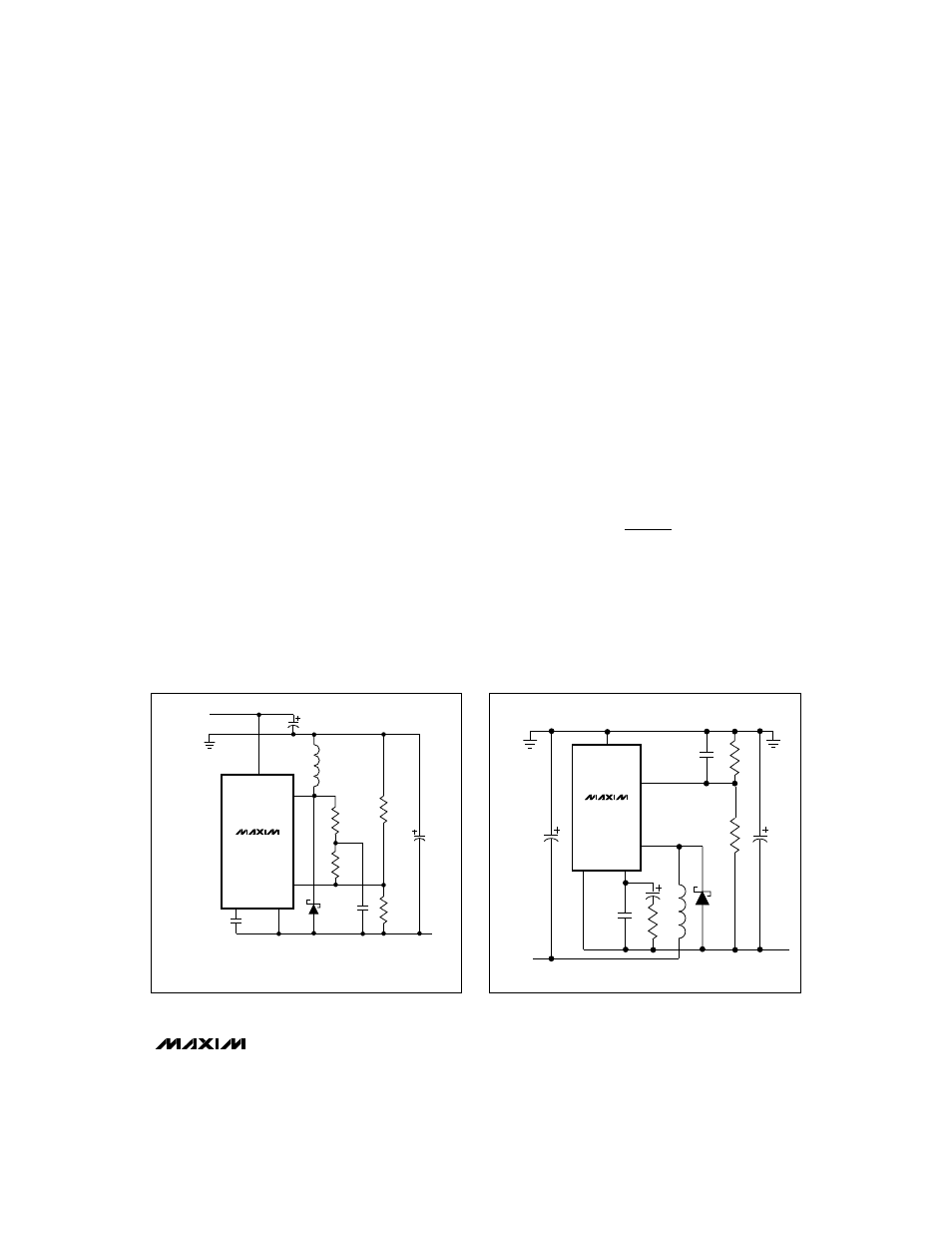
___________________Typical Applications
Positive-to-Negative DC-DC Inverter
The MAX724/MAX726 can convert positive input volt-
ages to negative outputs if the sum of input and output
voltage is greater than 8V, and the minimum positive
supply is 4.5V. The connection in Figure 7 shows the
MAX724 generating -5V. The device's GND pin is con-
nected to the negative output, which allows the feed-
back divider, R3, and R4 to be connected normally. If
the GND pin were tied to circuit ground, a level shift
and inversion would be required to generate the proper
feedback signal.
Component values in Figure 8 are shown for input volt-
ages up to 35V and for a 1A output. If the maximum
input voltage is lower, a Schottky diode with lower
reverse breakdown than the MBR745 (D1) may be
used. If lower output current is needed, then the cur-
rent rating of both D1 and L1 may be reduced. In addi-
tion, if the minimum input voltage is higher than 4.5V,
then greater output current can be supplied.
R1, R2, and C4 provide compensation for low input
voltages, but R1 and R2 also figure in the output-volt-
age calculation because they are effectively connected
in parallel with R3. For larger negative outputs,
increase R1, R2, and R3 proportionally while maintain-
ing the following relationships. If V
IN
does not fall below
2V
OUT
, then R1, R2, and C4 can be omitted and only R3
and R4 set the output voltage.
R4 = 1.82k
Ω
R3 = |V
OUT
| - 2.37 (in k
Ω
)
R1 = 1.86 (R3)
R2 = 3.65 (R3)
Negative Boost DC-DC Converter
The MAX724/MAX726 can also work as a negative
boost converter (Figure 8) by tying the GND pin to the
negative output. This allows the regulator to operate
from input voltages as low as -4.5V. If the regulated
output is at least -8V, R1 and R2 set the output volt-
age as in a conventional connection, with R1 selected
from:
R1 =
V
OUT
R2
- R2
2.21
L1 must be a low value to maintain stability, but if V
IN
is
greater than -10V, L1 can be increased to 50
µ
H. Since
this is a boost configuration, if the input voltage
exceeds the output voltage, D1 will pull the output more
negative and out of regulation. Also, if the output is
pulled toward ground, D1 will drag down the input sup-
ply. For this reason, this configuration is not short-cir-
cuit protected.
MAX724/MAX726
5A/2A Step-Down, PWM,
Switch-Mode DC-DC Regulators
______________________________________________________________________________________
11
D1 - MOTOROLA MBR745
C1 - NICHICON UPL1C221MRH6
C2 - NICHICON UPL1A102MRH6
L1 - COILTRONICS CTX25-5-52
MAX724
V
IN
+4.5V TO +35V
220
µ
H
50V
C1
L1
50
µ
H
5A
R1
5.1k
R2
10k
R3
2.74k
R4
1.82k
C2
1000
µ
F
10V
-5V
1A
C4
0.01
µ
F
D1
C3
0.1
µ
F
V
SW
V
IN
V
C
GND
FB
ALL RESISTORS HAVE 1% TOLERANCE
Figure 7. Positive-to-Negative DC-DC Inverter
MAX724
V
IN
R3
750
Ω
R2
2.21k
R1
12.7k
C1
1000
µ
F
25V
D1
MBR735
L1
25
µ
H
0.01
µ
F
GND
V
C
V
SW
FB
C3
100
µ
F
25V
1000pF
V
OUT
-15V
-V
IN
-4.5V TO -15V
C2
1
µ
F
Figure 8. Negative Step-Up DC-DC Converter