General dac discussion, Buffer amplifier – Rainbow Electronics MAX539 User Manual
Page 8
MAX531/MAX538/MAX539
+5V, Low-Power, Voltage-Output
Serial 12-Bit DACs
8
_______________________________________________________________________________________
10
FUNCTION
1
BIPOFF
Bipolar Offset/Gain
Resistor
2
DIN
Serial Data Input
3
CLR
Clear. Asynchronously sets
DAC register to 000 hex.
PIN
—
1
4
SCLK
Serial Clock Input
5
CS
Chip Select, active low
6
DOUT
Serial Data Output for
daisy-chaining
7
DGND
Digital Ground
—
2
3
8
AGND
Analog Ground
9
REFIN
Reference Input
4
—
5
6
—
REFOUT
Reference Output,
2.048V
11
—
V
SS
Negative Power Supply
12
7
VOUT
DAC Output
13
8
V
DD
Positive Power Supply
14
—
RFB
Feedback Resistor
MAX531
MAX538
MAX539
NAME
____________________Pin Description
_______________Detailed Description
General DAC Discussion
The MAX531/MAX538/MAX539 use an “inverted” R-2R
ladder network with a single-supply CMOS op amp to con-
vert 12-bit digital data to analog voltage levels (see
Functional Diagram)
. The term “inverted” describes the
ladder network because the REFIN pin in current-output
DACs is the summing junction, or virtual ground, of an op
amp. However, such use would result in the output voltage
being the inverse of the reference voltage. The
MAX531/MAX538/MAX539’s topology makes the output
the same polarity as the reference input.
An internal reset circuit forces the DAC register to reset to
000 hex on power-up. Additionally, a clear
CLR pin, when
held low, sets the DAC register to 000 hex.
CLR operates
asynchronously and independently from the chip-select
(
CS) pin.
Buffer Amplifier
The output buffer is a unity-gain stable, rail-to-rail output,
BiCMOS op amp. Input offset voltage and CMRR are
trimmed to achieve better than 12-bit performance.
Settling time is 25µs to 0.01% of final value. The settling
time is considerably longer when the DAC code is initially
set to 000 hex, because at this code the op amp is com-
pletely debiased. Start from code 001 hex if necessary.
The output is short-circuit protected and can drive a 2k
Ω
load with more than 100pF load capacitance.
t
CSH0
t
CSS
t
CH
t
CL
t
CSH1
t
CSW
t
DS
t
DH
t
DO
CS
SCLK
DIN
DOUT
t
CS1
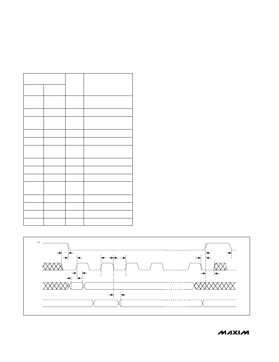
Figure 1. Timing Diagram