Rainbow Electronics MAX539 User Manual
Page 5
MAX531/MAX538/MAX539
+5V, Low-Power, Voltage-Output,
Serial 12-Bit DACs
_______________________________________________________________________________________
5
Note 2:
In single-supply operation, INL and GE calculated from code 11 to code 4095. Tested at V
DD
= +5V.
Note 3:
This specification applies to both gain-error power-supply rejection ratio and offset-error power-supply rejection ratio.
Note 4:
Guaranteed by design.
Note 5:
Tested at I
OUT
= 100µA. The reference can typically source up to 5mA (see
Typical Operating Characteristics
).
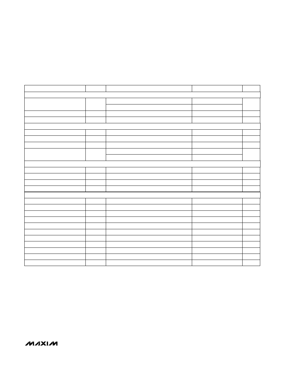
ELECTRICAL CHARACTERISTICS—Dual Supplies (MAX531 Only) (continued)
(V
DD
= +5V ±10%, V
SS
= -5V ±10%, AGND = DGND = 0V, REFIN = 2.048V (external), RFB = BIPOFF = VOUT, C
REFOUT
= 33µF,
R
L
= 10k
Ω
, C
L
= 100pF, T
A
= T
MIN
to T
MAX
, unless otherwise noted.)
PARAMETER
SYMBOL
MIN
TYP
MAX
UNITS
Voltage-Output Slew Rate
SR
dB
0.15
0.25
V
DD
V/µs
4.5
5.5
I
SC
12
V
mA
Positive Supply Voltage
1
LSB
Negative Supply Voltage
Voltage-Output Settling Time
25
µs
Signal-to-Noise plus Distortion
5
nV-s
V
SS
-5.5
0
V
Short-Circuit Current
68
Digital Feedthrough
SINAD
68
Output Load Regulation
V
SS
+ 2
V
DD
- 2
Output Voltage Range
V
SS
+ 0.4
V
DD
- 0.4
V
CONDITIONS
VOUT = 2V, R
L
= 2k
Ω
To ±1/2LSB, VOUT = 2V
Step 000 hex to FFF hex
REFIN = 1kHz, 2Vp-p, (G = +1)
REFIN = 1kHz, 2Vp-p, (G = +2)
MAX531 (G = +1)
MAX531 (G = +2)
CS Setup Time
t
CSS
20
ns
SCLK Fall to
CS Fall Hold Time
t
CSH0
15
ns
SCLK Fall to
CS Rise Hold Time
t
CSH1
0
ns
SCLK High Width
t
CH
35
ns
SCLK Low Width
t
CL
35
ns
DIN Setup Time
t
DS
45
ns
DIN Hold Time
t
DH
0
ns
DOUT Valid Propagation Delay
t
DO
C
L
= 50pF
80
ns
CS High Pulse Width
t
CSW
20
ns
CLR Pulse Width
t
CLR
25
ns
CS Rise to SCLK Rise Setup Time
t
CS1
50
ns
Positive Supply Current
I
DD
260
400
µA
All inputs = 0V or V
DD
, no load
Negative Supply Current
I
SS
-120
-200
µA
All inputs = 0V or V
DD
, no load
VOLTAGE OUTPUT (VOUT)
DYNAMIC PERFORMANCE
POWER SUPPLY
SWITCHING CHARACTERISTICS