Max1644, Design procedure, Table 1. recommended component values (i – Rainbow Electronics MAX1644 User Manual
Page 8: 2a, f, 300khz)
MAX1644
__________________Design Procedure
For typical applications, use the recommended compo-
nent values in Table 1. For other applications, take the
following steps:
1) Select the desired PWM-mode switching frequency;
300kHz is a good starting point.
2) Select the constant-off-time as a function of input
voltage, output voltage, and switching frequency.
3) Select R
TOFF
as a function of off-time.
4) Select the inductor as a function of output voltage,
off-time, and peak-to-peak inductor current.
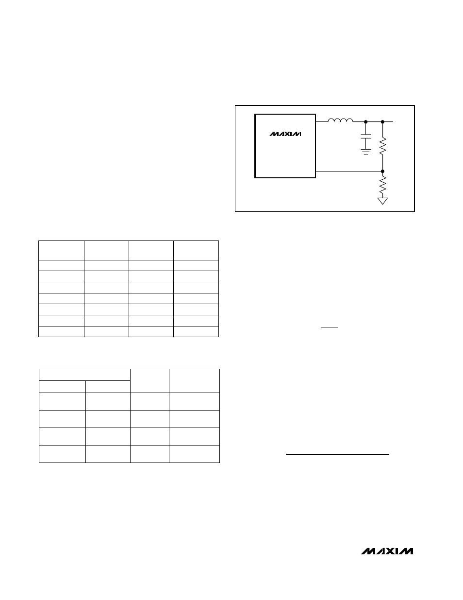
Setting the Output Voltage
The output of the MAX1644 is selectable between one
of two preset output voltages: (2.5V or 3.3V) with a 2%
AC load-regulation error, or an adjustable output volt-
age from the reference voltage (nominally 1.1V) up to
V
IN
with a 1% or 2% AC load-regulation error. For a
preset output voltage, connect FB to the output voltage,
and connect FBSEL to V
CC
(2.5V output voltage) or
leave unconnected (3.3V output voltage). Internal resis-
tor-dividers divide down the output voltage, regulating
the divided voltage to the internal reference voltage.
For output voltages other than 2.5V or 3.3V, or for
tighter AC load regulation, connect FBSEL to GND (1%
regulation) or to REF (2% regulation), and connect FB
to a resistor divider between the output voltage and
ground (Figure 2). Regulation is maintained for
adjustable output voltages when V
FB
equals V
REF
. Use
50k
Ω for R1. R2 is given by the equation:
where V
REF
is typically 1.1V.
Programming the Switching Frequency
and Off-Time
The MAX1644 features a programmable PWM mode
switching frequency, which is set by the input and out-
put voltage and the value of R
TOFF
, connected from
TOFF to GND. R
TOFF
sets the PMOS power switch off-
time in PWM mode. Use the following equation to select
the off-time according to your desired switching fre-
quency in PWM mode (I
OUT
> 0.2A):
where:
t
OFF
= the programmed off-time
V
IN
= the input voltage
V
OUT
= the output voltage
V
NMOS
= the voltage drop across the internal
PMOS power switch
V
PMOS
= the voltage drop across the internal
NMOS synchronous-rectifier switch
t
V
V
V
f
V
V
V
OFF
IN
OUT
PMOS
PWM
IN
PMOS
NMOS
–
=
−
(
)
−
+
(
)
R2
R1
V
V
1
OUT
REF
=
−
2A, Low-Voltage, Step-Down Regulator with
Synchronous Rectification and Internal Switches
8
_______________________________________________________________________________________
V
OUT
(V)
R
TOFF
(k
Ω)
6.0
120
L
(µH)
5
3.3
6.8
V
IN
(V)
180
6.8
240
5
1.8
3.3
82
3.3
2.5
4.7
180
3.3
1.8
4.7
200
3.3
1.5
5
2.5
Table 2. Output Voltage and AC Load-
Regulation Selection
PIN
2.5
2
V
CC
Output
Voltage
3.3
2
Adjustable
2
REF
Resistor
Divider
Adjustable
1
GND
Resistor
Divider
Unconnected
Output
Voltage
FB
AC LOAD-
REGULATION
ERROR (%)
OUTPUT
VOLTAGE
(V)
FBSEL
LX
R2
R1
R1 = 50k
Ω
R2 = R1(V
OUT
/ V
REF
- 1)
V
REF
= 1.1V
FB
V
OUT
MAX1644
Figure 2. Adjustable Output Voltage
Table 1. Recommended Component
Values (I
OUT
= 2A, f
PWM
= 300kHz)
6.0
270
5
1.5