Typical operating characteristics (continued), Pin description – Rainbow Electronics MAX1644 User Manual
Page 5
MAX1644
2A, Low-Voltage, Step-Down Regulator with
Synchronous Rectification and Internal Switches
_______________________________________________________________________________________
5
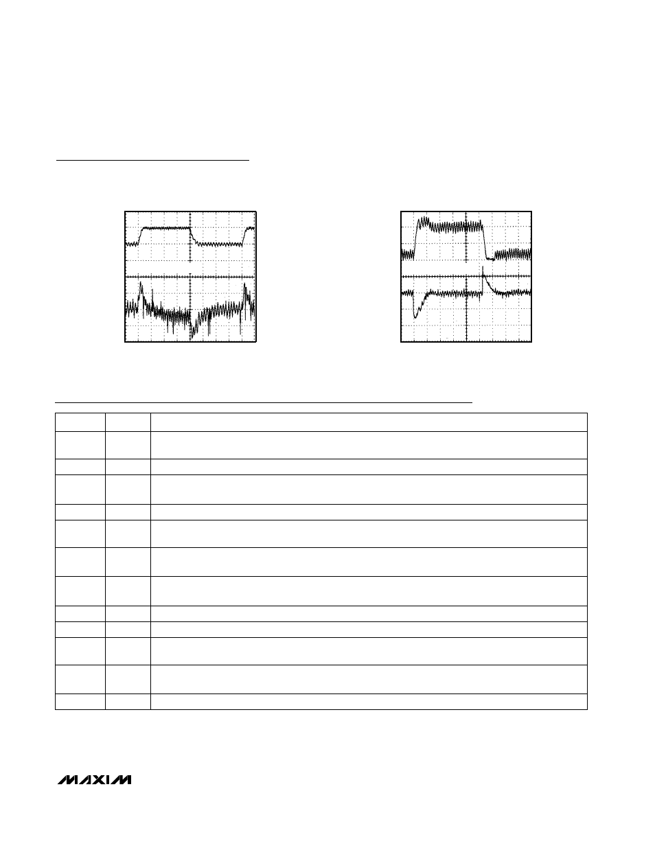
Typical Operating Characteristics (continued)
(Circuit of Figure 1, T
A
= +25°C, unless otherwise noted.)
NAME
FUNCTION
1
SHDN
Shutdown Control Input. Drive SHDN low to disable the reference, control circuitry, and internal
MOSFETs. Drive high or connect to V
CC
for normal operation.
PIN
Pin Description
V
IN
V
OUT
20mV/div
4V
3V
20
µs/div
LINE-TRANSIENT RESPONSE
MAX1644-10
V
OUT
= 1.5V, I
OUT
= 2A
I
L
V
OUT
50mV/div
2A
0
20
µs/div
LOAD-TRANSIENT RESPONSE
(FBSEL = REF)
MAX1644-11
V
IN
= 3.3V, V
OUT
= 1.5V
2, 4
IN
Supply Voltage Input for the internal PMOS power switch
3, 14, 16
LX
Connection for the drains of the PMOS power switch and NMOS synchronous-rectifier switch. Connect
the inductor from this node to output filter capacitor and load.
5
SS
Soft-Start. Connect a capacitor from SS to GND to limit inrush current during start-up.
6
COMP
Integrator Compensation. Connect a capacitor from COMP to V
CC
for integrator compensation. See the
Integrator Amplifier section.
7
TOFF
Off-Time Select Input. Sets the PMOS power switch off-time during constant-off-time operation. Connect a
resistor from TOFF to GND to adjust the PMOS switch off-time.
8
FB
Feedback Input for both preset-output and adjustable-output operating modes. Connect directly to
output for fixed-voltage operation or to a resistor-divider for adjustable operating modes.
9
GND
Analog Ground
10
REF
Reference Output. Bypass REF to GND with a 1µF capacitor.
11
FBSEL
Feedback Select Input. Selects AC load-regulation error and output voltage. See Table 2 for program-
ming instructions.
12
V
CC
Analog Supply Voltage Input. Supplies internal analog circuitry. Bypass V
CC
with a 10
Ω and 2.2µF low-
pass filter. See Figure 1.
13, 15
PGND
Power Ground. Internally connected to the internal NMOS synchronous-rectifier switch.