Rainbow Electronics MAX1644 User Manual
Page 7
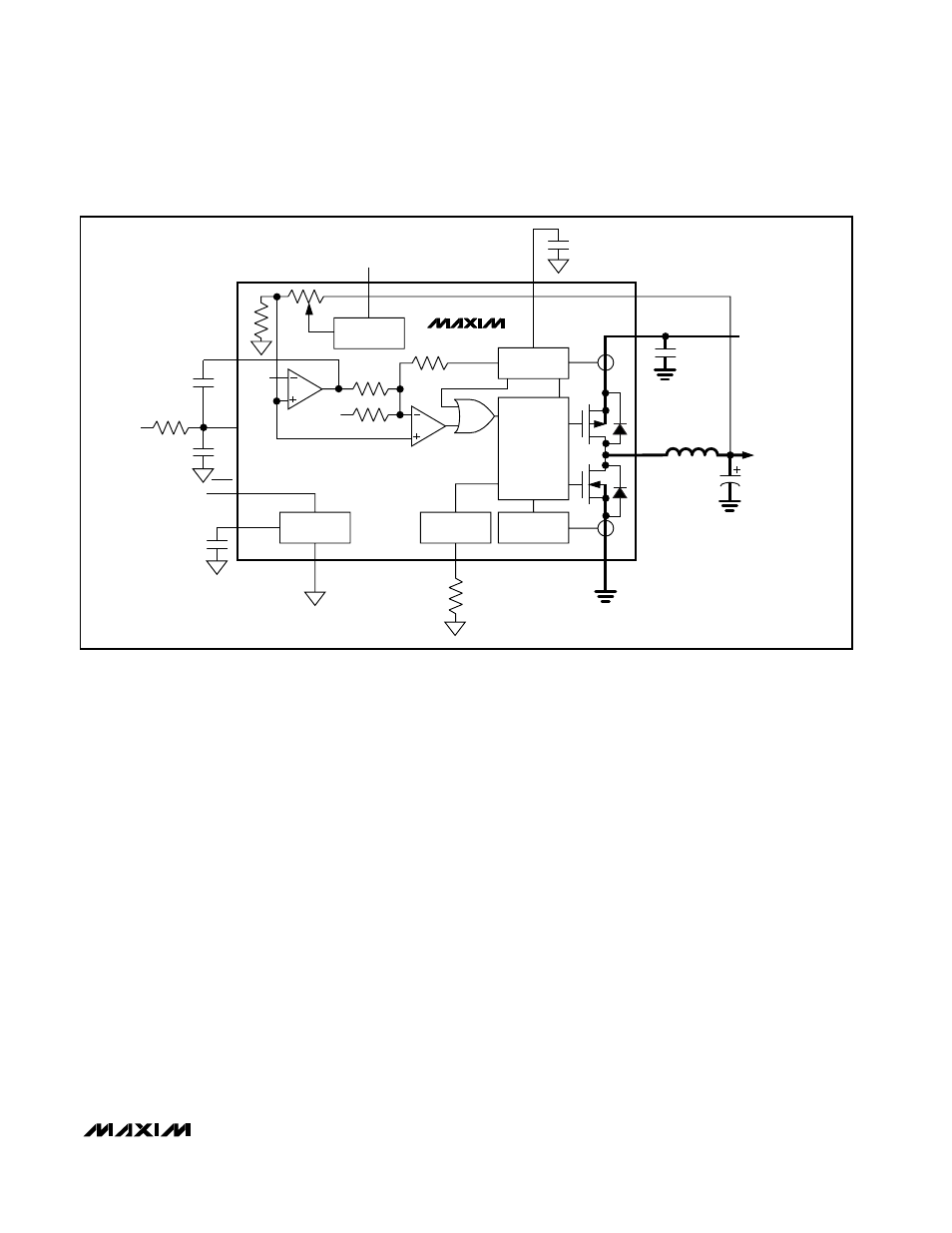
Synchronous Rectification
In a step-down regulator without synchronous rectifica-
tion, an external Schottky diode provides a path for cur-
rent to flow when the inductor is discharging. Replacing
the Schottky diode with a low-resistance NMOS syn-
chronous switch reduces conduction losses and
improves efficiency.
The NMOS synchronous-rectifier switch turns on follow-
ing a short delay after the PMOS power switch turns off,
thus preventing cross conduction or “shoot through.” In
constant-off-time mode, the synchronous-rectifier
switch turns off just prior to the PMOS power switch
turning on. While both switches are off, inductor current
flows through the internal body diode of the NMOS
switch. The internal body diode’s forward voltage is rel-
atively high.
Thermal Resistance
Junction-to-ambient thermal resistance,
θ
JA
, is highly
dependent on the amount of copper area immediately
surrounding the IC leads. The MAX1644 evaluation kit
has 0.5 in.
2
of copper area and a thermal resistance of
60°C/W with no airflow. Airflow over the IC significantly
reduces the junction-to-ambient thermal resistance. For
heatsinking purposes, evenly distribute the copper area
connected at the IC among the high-current pins.
Power Dissipation
Power dissipation in the MAX1644 is dominated by
conduction losses in the two internal power switches.
Power dissipation due to supply current in the control
section and average current used to charge and dis-
charge the gate capacitance of the internal switches
are less than 30mW at 300kHz. This number is reduced
when the switching frequency decreases as the part
enters Idle Mode. Combined conduction losses in the
two power switches are approximated by:
P
D
= I
OUT2
· R
ON
The junction-to-ambient thermal resistance required to
dissipate this amount of power is calculated by:
θ
JA
= (T
J,MAX
- T
A,MAX
) / P
D
where:
θ
JA
= junction-to-ambient thermal resistance
T
J,MAX
= maximum junction temperature
T
A,MAX
= maximum ambient temperature
MAX1644
2A, Low-Voltage, Step-Down Regulator with
Synchronous Rectification and Internal Switches
_______________________________________________________________________________________
7
MAX1644
V
CC
470pF
2.2
µF
1
µF
10
µF
10
Ω
FBSEL
0.01
µF
FEEDBACK
SELECTION
CURRENT
SENSE
PWM LOGIC
AND
DRIVERS
SS
IN
FB
V
IN
3.0V TO 5.5V
LX
PGND
TOFF
R
TOFF
GND
NOTE: HEAVY LINES DENOTE HIGH-CURRENT PATHS.
REF
REF
SUMMING
COMPARATOR
REF
REF
COMP
SKIP
SHDN
TIMER
V
IN
CURRENT
SENSE
G
m
C
OUT
V
OUT
Figure 1. Functional Diagram