Rainbow Electronics MAX970 User Manual
Page 10

MAX965–MAX970
Single/Dual/Quad, Micropower,
Ultra-Low-Voltage, Rail-to-Rail I/O Comparators
10
______________________________________________________________________________________
HYST
REF
GND
V
CC
R1
R2
MAX965
MAX967
MAX968
MAX969
+1.6V TO +5.5V
I
REF
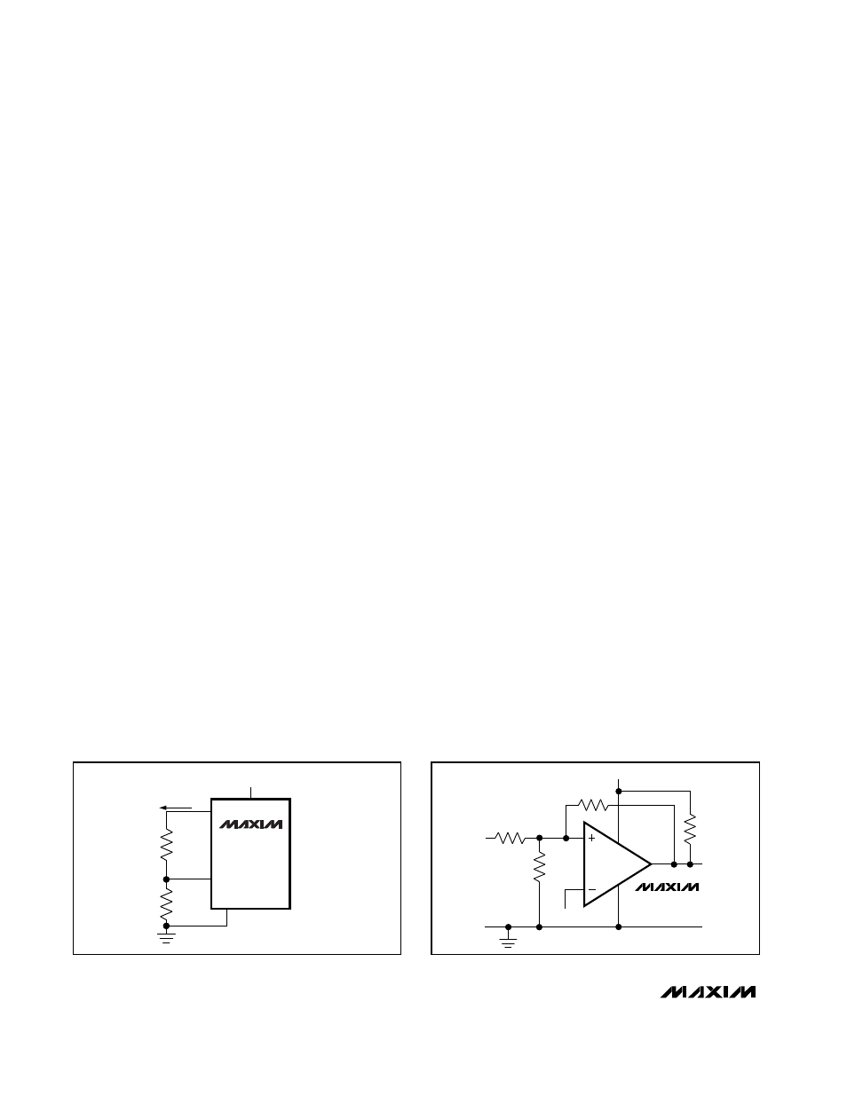
Figure 3. Programming the HYST Pin
GND
V
CC
V
CC
OUT
R3
R1
R2
R4
V
REF
V
IN
MAX966
MAX970
Figure 4. External Hysteresis
Figure 2 illustrates the case in which IN- has a fixed
voltage applied, and IN+ is varied. If the inputs were
reversed, the figure would be the same, except with an
inverted output.
Adding Hysteresis to the
MAX965/MAX967/MAX968/MAX969
To add hysteresis to the MAX965/MAX967/MAX968/
MAX969, connect resistor R1 between REF and HYST,
and connect resistor R2 between HYST and GND
(Figure 3). If additional hysteresis is not required,
connect HYST to REF. When hysteresis is added, the
upper and lower trip points change by the same
amount in opposite directions. The hysteresis band (the
difference between the upper and lower trip points,
V
HB
) is approximately twice the voltage between HYST
and REF. The HYST input voltage range is from REF
down to (REF - 50mV). This yields a hysteresis band
from ±1mV to a maximum of ±50mV. Calculate the val-
ues of R1 and R2 for the desired hysteresis band with
the following formulas:
R1 = V
HB
/ I
REF
R2 = (V
REF
- V
HB
) / I
REF
where I
REF
(the current sourced by the reference) does
not exceed the REF source capability (12µA typical),
and is significantly larger than the HYST leakage cur-
rent (5nA typical). I
REF
values between 0.1µA and 4µA
are good choices. If 2.4M
Ω
is chosen for R2 (I
REF
=
0.5µA), the equation for R1 and V
HB
can be approxi-
mated as:
R1(k
Ω
) = 2 x V
HB
(mV)
In the MAX967/MAX968/MAX969, the HYST pin pro-
grams the same hysteresis for all comparators in the
package.
Due to the internal structure of the input developed for
ultra-low-voltage operation, the hysteresis band varies
with common-mode voltage. The graph Programmed
Hysteresis vs. Common-Mode Voltage in the Typical
Operating Characteristics shows this variation. Notice
that the hysteresis band increases to almost twice the
calculated value toward the ends of the common-mode
range. This is apparent only when programming addi-
tional hysteresis using the HYST pin. The hysteresis
band is constant when HYST is connected to REF.
Adding Hysteresis to the MAX966/MAX970
The MAX966/MAX970 do not have a HYST pin for pro-
gramming hysteresis. Hysteresis can be generated with
three resistors using positive feedback (Figure 4). This
method generally draws more current than the method
using the HYST pin on the MAX965/MAX967/MAX968/
MAX969. Also, the positive feedback method slows
hysteresis response time. Use the following procedure
to calculate the resistor values:
1) Select R3. The leakage current of IN+ is under 5nA,
so the current through R3 should be at least 500nA
to minimize errors caused by leakage current. The
current through R3 at the trip point is (V
REF
- V
OUT
) /
R3. Taking into consideration the two possible out-
put states and solving for R3 yields two formulas:
R3 = V
REF
/ 500nA
and
R3 = (V
REF
- V
CC
) / 500nA
Use the smaller of the two resulting resistor values.
For example, if V
REF
= 1.2V and V
CC
= 5.0V, then
the two resistor values are 2.4M
Ω
and 7.6m
Ω
. For
R3, choose the 2.2M
Ω
standard value.
2) Choose the hysteresis band required (V
HB
). For this
example, choose 50mV.
