Rainbow Electronics MAX685 User Manual
Page 2
MAX685
Dual-Output (Positive and Negative),
DC-DC Converter for CCD and LCD
2
_______________________________________________________________________________________
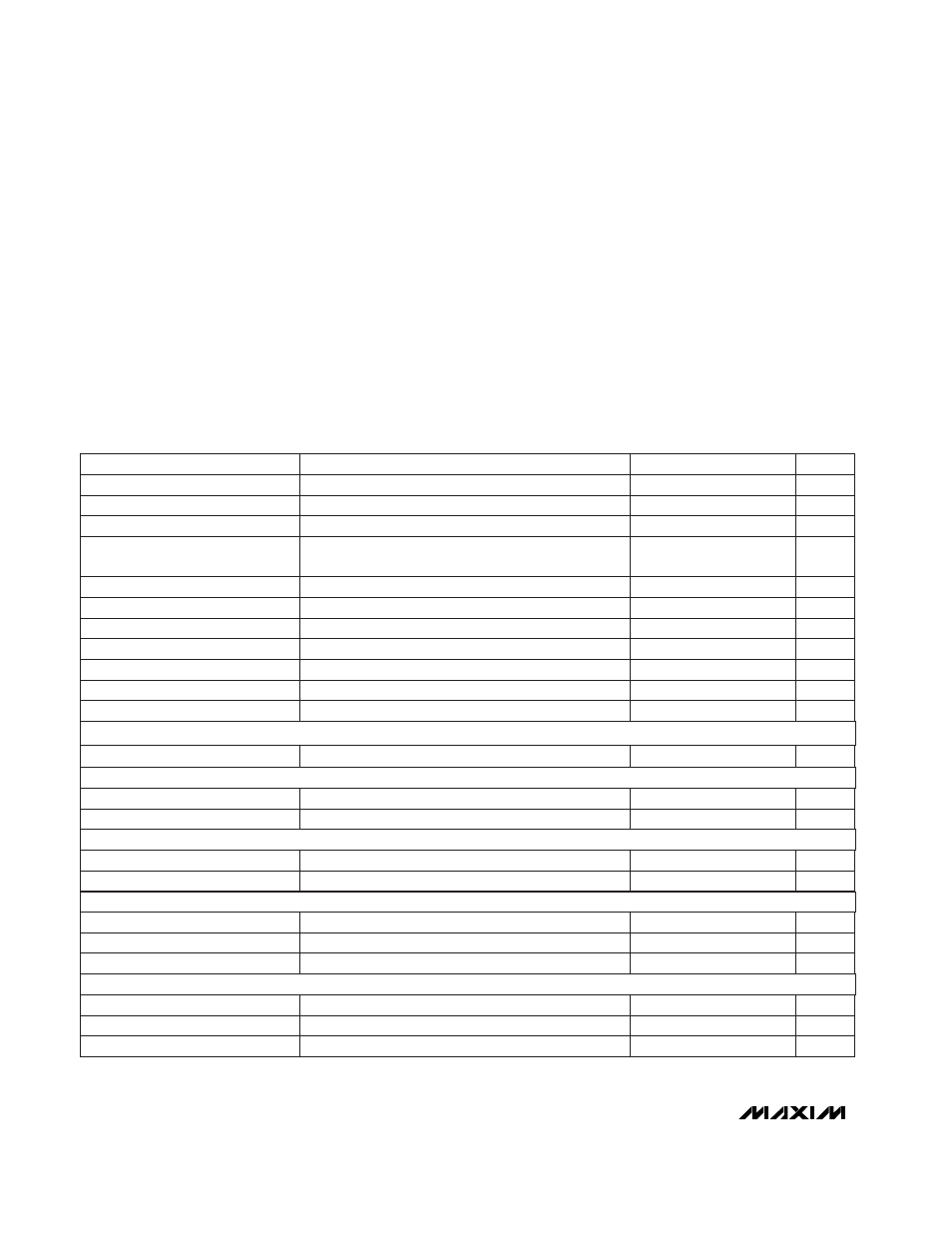
ABSOLUTE MAXIMUM RATINGS
ELECTRICAL CHARACTERISTICS
(V
DD
= VP = 5V,
T
A
= 0°C to +85°C
unless otherwise noted. Typical values are at T
A
= +25°C.)
Stresses beyond those listed under “Absolute Maximum Ratings” may cause permanent damage to the device. These are stress ratings only, and functional
operation of the device at these or any other conditions beyond those indicated in the operational sections of the specifications is not implied. Exposure to
absolute maximum rating conditions for extended periods may affect device reliability.
V
DD
, VP to GND........................................................-0.3V to +6V
PGND to GND .......................................................-0.3V to +0.3V
V
DD
to VP...............................................................-0.3V to +0.3V
LXN, POK to GND ..................................................-0.3V to +30V
LXP to V
DD
..............................................................-15V to +0.3V
REF, SEQ,
SHDN to GND...........................-0.3V to (V
DD
+ 0.3V)
FBP, FBN, SYNC to GND .........................................-0.3V to +6V
Continuous Power Dissipation (T
A
= +70°C)
16-Pin QSOP (derate 8.3mW/°C above +70°C)............667mW
Operating Temperature Range ...........................-40°C to +85°C
Junction Temperature ......................................................+150°C
Storage Temperature Range .............................-65°C to +165°C
Lead Temperature (soldering, 10sec) .............................+300°C
2.7V < V
DD
< 5.5V
2.7V < V
DD
< 5.5V
V
DD
= 5.5V (Note 1)
No load
V
DD
= VP
No load
C3 = C4 = 10µF, I
LOAD
= 5mA
I
OUT
= 0 to 10mA, C1 = 10µF
V
DD
= rising
V
DD
= 4.5V to 5.5V
V
FBP
= 1.35V, V
FBN
= -0.1V
V
DD
= 4.5V, V
OUT+
≥
14.25V, V
OUT-
≤
-7.125V,
Figure 3
T
A
= +25°C
V
DD
= 4.5V
SYNC = SEQ = SHDN = GND
SYNC = V
DD
CONDITIONS
µA
0.1
1
Input Bias Current
V
0.7 x V
DD
Logic-High Input
V
0.3 x V
DD
Logic-Low Input
µA
±0.01
±0.1
FBP, FBN Input Leakage Current
mV
-16
10
36
FBN Threshold Voltage
V
1.21
1.24
1.27
FBP Threshold Voltage
mV
50
UVLO Hysteresis
V
2.35
2.5
2.65
UVLO Threshold
µA
0.1
10
Shutdown Supply Current
V
-9
-1.27
Negative Output Voltage Range
V
VP
24
V
2.7
5.5
Input Voltage Range
Positive Output Voltage Range
mVp-p
30
Output Voltage Ripple
%/mA
0.13
Load Regulation
%/V
0.2
Line Regulation
µA
300
500
Idle Quiescent Current
mA
10
Output Current
mA
440
LX Current Limit
Ω
0.6
2
LXP, LXN On-Resistance
mA
0.8
Quiescent Current
UNITS
MIN
TYP
MAX
PARAMETER
0 < I
REF
< 50µA
No load
mV
-2
V
REF
Load Regulation
V
1.23
1.250
1.27
V
REF
Output Voltage
SHUTDOWN (
SHDN
)
UNDERVOLTAGE LOCKOUT
REFERENCE VOLTAGE
FB INPUTS
LOGIC INPUTS
(SEQ, SHDN, SYNC)