Note 1), Note 2), Note 3) – Rainbow Electronics LM75 User Manual
Page 5: Note 4), Logic electrical characteristics, Lm75
Logic Electrical Characteristics
(Continued)
DIGITAL DC CHARACTERISTICS Unless otherwise noted, these specifications apply for +V
S
= +5 Vdc for LM75BIM-5,
LM75BIMM-5, LM75CIM-5, and LM75CIMM-5 and +V
S
= +3.3 Vdc for LM75BIM-3, LM75BIMM-3, LM75CIM-3, and
LM75CIMM-3 (Note 6). Boldface limits apply for T
A
= T
J
= T
MIN
to T
MAX
; all other limits T
A
= T
J
= +25˚C, unless otherwise
noted.
Symbol
Parameter
Conditions
Typical
Limits
Units
(Limit)
t
OF
Output Fall Time
C
L
= 400 pF
250
ns (max)
I
O
= 3 mA
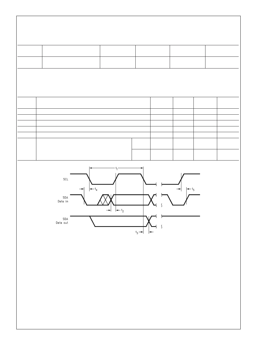
I
2
C DIGITAL SWITCHING CHARACTERISTICS Unless otherwise noted, these specifications apply for +V
S
= +5 Vdc for
LM75BIM-5, LM75BIMM-5, LM75CIM-5, and LM75CIMM-5 and +V
S
= +3.3 Vdc for LM75BIM-3, LM75BIMM-3, LM75CIM-3,
and LM75CIMM-3. C
L
(load capacitance) on output lines = 80 pF unless otherwise specified. Boldface limits apply for T
A
=
T
J
= T
MIN
to T
MAX
; all other limits T
A
= T
J
= +25˚C, unless otherwise noted. The switching characteristics of the LM75 fully
meet or exceed the published specifications of the I
2
C bus. The following parameters are the timing relationships between SCL
and SDA signals related to the LM75. They are not the I
2
C bus specifications.
Symbol
Parameter
Conditions
Typical
Limits
Units
(Limit)
t
1
SCL (Clock) Period
2.5
µs (min)
t
2
Data in Set-Up Time to SCL High
100
ns (min)
t
3
Data Out Stable after SCL Low
0
ns (min)
t
4
SDA Low Set-Up Time to SCL Low (Start Condition)
100
ns (min)
t
5
SDA High Hold Time after SCL High (Stop Condition)
100
ns (min)
t
TIMEOUT
SDA Time Low for Reset of Serial Interface (Note 13)
LM75B
75
325
ms (min)
ms (max)
LM75C
Not
Applicable
01265804
Note 1: Absolute Maximum Ratings indicate limits beyond which damage to the device may occur. DC and AC electrical specifications do not apply when operating
the device beyond its rated operating conditions.
Note 2: When the input voltage (V
I
) at any pin exceeds the power supplies (V
I
<
GND or V
I
>
+V
S
) the current at that pin should be limited to 5 mA. The 20 mA
maximum package input current rating limits the number of pins that can safely exceedthe power supplies with an input current of 5 mA to four.
Note 3: See AN-450 “Surface Mounting Methods and Their Effect on Product Reliability” or the section titled “Surface Mount” found in a current National
Semiconductor Linear Data Book for other methods of soldering surface mount devices.
Note 4: Human body model, 100 pF discharged through a 1.5 k
Ω resistor. Machine model, 200 pF discharged directly into each pin.
LM75
www.national.com
5