10 internal register structure, 0 functional description, Lm75 – Rainbow Electronics LM75 User Manual
Page 10
1.0 Functional Description
(Continued)
1.10 INTERNAL REGISTER STRUCTURE
01265808
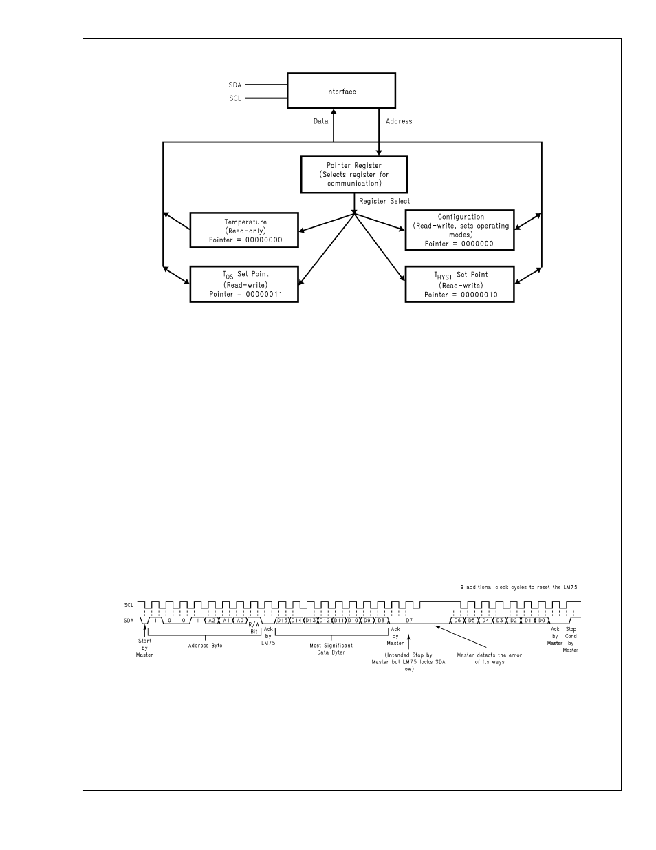
There are four data registers in the LM75, selected by the
Pointer register. At power-up the Pointer is set to “00”; the
location for the Temperature Register. The Pointer register
latches whatever the last location it was set to. In Interrupt
Mode, a read from the LM75, or placing the device in shut-
down mode, resets the O.S. output. All registers are read
and write, except the Temperature register which is read
only.
A write to the LM75 will always include the address byte and
the Pointer byte. A write to the Configuration register re-
quires one data byte, and the T
OS
and T
HYST
registers
require two data bytes.
Reading the LM75 can take place either of two ways: If the
location latched in the Pointer is correct (most of the time it is
expected that the Pointer will point to the Temperature reg-
ister because it will be the data most frequently read from the
LM75), then the read can simply consist of an address byte,
followed by retrieving the corresponding number of data
bytes. If the Pointer needs to be set, then an address byte,
pointer byte, repeat start, and another address byte will
accomplish a read.
The first data byte is the most significant byte with most
significant bit first, permitting only as much data as neces-
sary to be read to determine temperature condition. For
instance, if the first four bits of the temperature data indi-
cates an overtemperature condition, the host processor
could immediately take action to remedy the excessive tem-
peratures. At the end of a read, the LM75 can accept either
Acknowledge or No Acknowledge from the Master (No Ac-
knowledge is typically used as a signal for the slave that the
Master has read its last byte).
An inadvertent 8-bit read from a 16-bit register, with the D7
bit low, can cause the LM75 to stop in a state where the SDA
line is held low as shown in Figure 5. This can prevent any
further bus communication until at least 9 additional clock
cycles have occurred. Alternatively, the master can issue
clock cycles until SDA goes high, at which time issuing a
“Stop” condition will reset the LM75.
01265809
FIGURE 5. Inadvertent 8-Bit Read from 16-Bit Register where D7 is Zero (“0”)
LM75
www.national.com
10