Detailed description, Pin description – Rainbow Electronics MAX1273 User Manual
Page 8

MAX1272/MAX1273
Detailed Description
Converter Operation
The MAX1272/MAX1273 multirange ADCs use succes-
sive approximation and internal track/hold (T/H) circuitry
to convert an analog signal to a 12-bit digital output.
Figure 2 shows a block diagram of the MAX1272/
MAX1273.
Analog-Input Track/Hold
The T/H tracking/acquisition mode begins on the falling
edge of the fourth clock cycle in the 8-bit input control
word and enters hold/conversion mode on the falling
edge of the eighth clock cycle.
The MAX1272/MAX1273 input architecture includes a
resistor-divider and a T/H system (Figure 3). When
operating in bipolar or unipolar mode, the resistor-
divider network formed by R1, R2, and R3 scales the
signal applied at the input channel. Use a low source
impedance (<4
Ω) to minimize gain error.
Input Bandwidth
The ADC’s small-signal input bandwidth depends on
the selected input range and varies from 1.25MHz to
5MHz (see the Electrical Characteristics). The maxi-
mum sampling rate for the MAX1272/MAX1273 is
87ksps (16 clocks per conversion). Use undersampling
techniques to digitize high-speed transient events and
measure periodic signals with bandwidths exceeding
the ADC’s sampling rate.
Use anti-alias filtering to avoid the aliasing of high-fre-
quency signals into the frequency band of interest. An
anti-aliasing filter must limit the input bandwidth to no
more than one half of the sampling frequency.
Fault-Protected, 12-Bit ADCs
with Software-Selectable Input Range
8
_______________________________________________________________________________________
Pin Description
PIN
NAME
FUNCTION
1
SCLK
Serial Clock Input. Clocks data in and out of serial interface. SCLK sets the conversion speed.
2
DIN
Serial Data Input. Data clocks in on the rising edge of SCLK.
3
V
DD
5V Supply. Bypass with a 0.1µF capacitor to GND.
4
GND
Ground
5
AIN
Analog Input
6
REF
Reference Buffer Output/Reference Input. Bypass REF with a 1µF capacitor to GND. In internal
reference mode, the reference buffer provides a 4.096V nominal output. For external reference mode,
disable the internal reference buffer through the serial interface and apply an external reference to REF.
7
CS
Active-Low Chip-Select Input. Drive
CS low to clock data into the MAX1272/MAX1273. See the Input
Data Format section.
8
DOUT
Serial Data Output. Data clocks out on the falling edge of SCLK. DOUT is high impedance when
CS is
high.
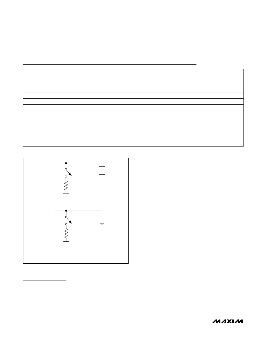
A) TEST CIRCUIT FOR V
OH
1k
Ω
DOUT
C
LOAD
B) TEST CIRCUIT FOR V
OL
1k
Ω
DOUT
C
LOAD
5V
f
SCLK
= 1.4MHz, C
LOAD
= 50pF
Figure 1. Output Load Circuit for Timing Characteristics
