Table 4. power-down selection – Rainbow Electronics MAX1273 User Manual
Page 10
MAX1272/MAX1273
Input Data Format
Input data (control byte) clocks in at DIN on the rising
edge of SCLK. CS enables communication with the
MAX1272/MAX1273. After CS falls, the first arriving 1
represents the start bit (MSB) of the input control byte.
The start bit is defined as follows:
1) The first high bit clocked into DIN with CS low any
time the converter is idle (e.g., after applying V
DD
).
2) The first high bit clocked into DIN after bit 4 (D4) of a
conversion in progress clocks out on DOUT.
See Table 1 for programming the control byte. Figure 4
shows the detailed serial interface timing.
Output Data Format
Output data (DOUT) clocks out MSB first on the falling
edge of SCLK. The unipolar mode provides a straight
binary output. The bipolar mode provides a two’s com-
plement binary output. For output binary codes, see the
Transfer Function section.
Fault-Protected, 12-Bit ADCs
with Software-Selectable Input Range
10
______________________________________________________________________________________
INPUT RANGE
RNG
BIP
NEGATIVE
FULL SCALE
ZERO SCALE
FULL SCALE
0 to 5V
0
0
—
0
V
REF
× 1.2207
±
5V
0
1
-V
REF
× 1.2207
0
V
REF
× 1.2207
0 to 10V
1
0
—
0
V
REF
× 2.4414
±
10V
1
1
-V
REF
× 2.4414
0
V
REF
× 2.4414
Table 2. Input Range and Polarity Selection for MAX1272
INPUT RANGE
RNG
BIP
NEGATIVE
FULL SCALE
ZERO SCALE
FULL SCALE
0 to V
REF
/ 2
0
0
—
0
V
REF
/ 2
±
V
REF
/ 2
0
1
-V
REF
/ 2
0
V
REF
/ 2
0 to V
REF
1
0
—
0
V
REF
±
V
REF
1
1
-V
REF
0
V
REF
Table 3. Input Range and Polarity Selection for MAX1273
PD
MODE1
MODE0
MODE
1
X
X
Normal operation (ADCs always active). Automatically enters delayed
standby power-down mode between conversions.
0
Delayed standby power-down mode.
0
1
Immediate standby power-down mode.
0
Delayed full power-down mode.
0
1
1
Immediate full power-down mode.
Table 4. Power-Down Selection
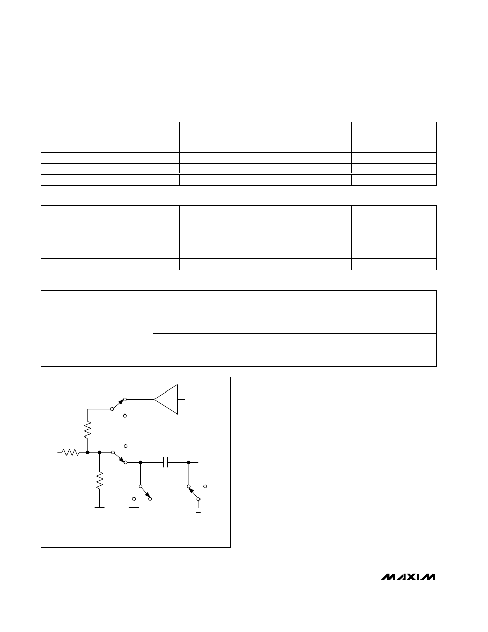
R3
4.8k
Ω
R2
R1
AIN
S1
S2
S3
S4
BIPOLAR
UNIPOLAR
VOLTAGE
REFERENCE
T/H
OUT
HOLD
TRACK
TRACK
HOLD
OFF
ON
C
HOLD
S1 = BIPOLAR/UNIPOLAR SWITCH
S2 = INPUT MUX SWITCH
S3, S4 = T/H SWITCH
R1 = 11.3k
Ω (MAX1272)
or 4.8k
Ω (MAX1273)
R2 = 7.8k
Ω (MAX1272)
or
∞ (OPEN) (MAX1273)
Figure 3. Equivalent Input Circuit