Rainbow Electronics MAX782 User Manual
Page 13
MAX782
Triple-Output Power-Supply
Controller for Notebook Computers
______________________________________________________________________________________
13
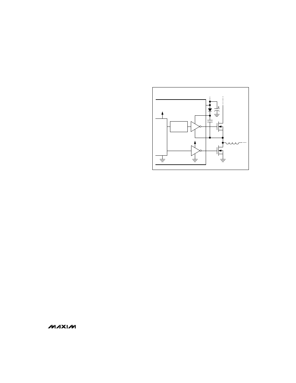
Boost Gate-Driver Supply
Gate-drive voltage for the high-side N-channel switch is
generated with a flying-capacitor boost circuit as shown
in Figure 4. The capacitor is alternately charged from
the VL supply via the diode and placed in parallel with
the high-side MOSFET’s gate-source terminals. On start-
up, the synchronous rectifier (low-side) MOSFET forces
LX_ to 0V and charges the BST_ capacitor to 5V. On the
second half-cycle, the PWM turns on the high-side
MOSFET by connecting the capacitor to the MOSFET
gate by closing an internal switch between BST_ and
DH_. This provides the necessary enhancement voltage
to turn on the high-side switch, an action that “boosts”
the 5V gate-drive signal above the battery voltage.
Ringing seen at the high-side MOSFET gates (DH3 and
DH5) in discontinuous-conduction mode (light loads) is
a natural operating condition caused by the residual
energy in the tank circuit formed by the inductor and
stray capacitance at the LX_ nodes. The gate driver
negative rail is referred to LX_, so any ringing there is
directly coupled to the gate-drive supply.
Modes of Operation
PWM Mode
Under heavy loads – over approximately 25% of full load
– the +3.3V and +5V supplies operate as continuous-cur-
rent PWM supplies (see
Typical Operating
Characteristics). The duty cycle (%ON) is approximately:
%ON = V
OUT
/V
IN
Current flows continuously in the inductor: First, it
ramps up when the power MOSFET conducts; then, it
ramps down during the flyback portion of each cycle
as energy is put into the inductor and then dis-
charged into the load. Note that the current flowing
into the inductor when it is being charged is also
flowing into the load, so the load is continuously
receiving current from the inductor. This minimizes
output ripple and maximizes inductor use, allowing
very small physical and electrical sizes. Output rip-
ple is primarily a function of the filter capacitor (C7 or
C6) effective series resistance (ESR) and is typically
under 50mV (see the
Design Procedure section).
Output ripple is worst at light load and maximum
input voltage.
Idle Mode
Under light loads (<25% of full load), efficiency is fur-
ther enhanced by turning the drive voltage on and off
for only a single clock period, skipping most of the
clock pulses entirely. Asynchronous switching, seen as
“ghosting” on an oscilloscope, is thus a normal operating
condition whenever the load current is less than
approximately 25% of full load.
At certain input voltage and load conditions, a transition
region exists where the controller can pass back and
forth from idle-mode to PWM mode. In this situation,
short bursts of pulses occur that make the current
waveform look erratic, but do not materially affect the
output ripple. Efficiency remains high.
Current Limiting
The voltage between CS3 (CS5) and FB3 (FB5) is contin-
uously monitored. An external, low-value shunt resistor is
connected between these pins, in series with the induc-
tor, allowing the inductor current to be continuously mea-
sured throughout the switching cycle. Whenever this
voltage exceeds 100mV, the drive voltage to the external
high-side MOSFET is cut off. This protects the MOSFET,
the load, and the battery in case of short circuits or tem-
porary load surges. The current-limiting resistor R1 (R2)
is typically 25m
Ω
(20m
Ω
) for 3A load current.
Oscillator Frequency; SYNC Input
The SYNC input controls the oscillator frequency.
Connecting SYNC to GND or to VL selects 200kHz opera-
tion; connecting to REF selects 300kHz operation. SYNC
can also be driven with an external 240kHz to 350kHz
CMOS/TTL source to synchronize the internal oscillator.
Normally, 300kHz is used to minimize the inductor and
filter capacitor sizes, but 200kHz may be necessary for
low input voltages (see
Low-Voltage (6-cell) Operation).
LEVEL
TRANSLATOR
PWM
VL
BST_
DH_
LX_
DL_
VL
BATTERY
INPUT
VL
Figure 4. Boost Supply for Gate Drivers