Rainbow Electronics MAX1643 User Manual
Page 9
MAX1642/MAX1643
High-Efficiency, Step-Up
DC-DC Converters for 1V Inputs
_______________________________________________________________________________________
9
Capacitor Selection
Choose input and output capacitors to service input
and output peak currents with acceptable voltage rip-
ple. A 22µF, 6V, low-ESR, surface-mount tantalum out-
put filter capacitor typically provides 60mV output
ripple when stepping up from 1.3V to 3.3V at 20mA.
The input filter capacitor (C
IN
) also reduces peak cur-
rents drawn from the battery and improves efficiency.
Low equivalent series resistance (ESR) capacitors are
recommended. Capacitor ESR is a major contributor to
output ripple (usually more than 60%). Ceramic capaci-
tors have the lowest ESR, but low-ESR tantalums repre-
sent a good balance between cost and performance.
Low-ESR aluminum electrolytic capacitors are tolerable,
and standard aluminum electrolytic capacitors should
be avoided. Do not exceed tantalum capacitors’ ripple-
current ratings; select capacitors with a rating exceed-
ing the peak inductor current (I
PEAK
).
PC Board Layout and Grounding
High switching frequencies and large peak currents
make PC board layout an important part of design. Poor
design can result in excessive EMI on the feedback paths
and voltage gradients in the ground plane. Both of these
factors can result in instability or regulation errors. The
OUT pin must be bypassed directly to GND as close to
the IC as possible (within 0.2 in. or 5mm).
Place power components—such as the MAX1642/
MAX1643, inductor, input filter capacitor, and output filter
capacitor—as close together as possible. Keep their
traces short, direct, and wide (
≥
50 mil or 1.25mm), and
place their ground pins close together in a star-ground
configuration. Keep the extra copper on the board and
integrate it into ground as a pseudo-ground plane. On
multilayer boards, route the star ground using compo-
nent-side copper fill, then connect it to the internal ground
plane using vias.
Place the external voltage-feedback network very close to
the FB pin (within 0.2 in. or 5mm). Noisy traces, such as
from the LX pin, should be kept away from the voltage-
feedback network and separated from it using grounded
copper. The evaluation kit manual shows an example PC
board layout, routing, and pseudo-ground plane.
Noise and Voltage Ripple
EMI and output voltage ripple can be minimized by fol-
lowing a few simple design rules.
1) Place the DC-DC converter and digital circuitry on
an opposite corner of the PC board, away from sen-
sitive RF and analog input stages.
2) Use a closed-core inductor, such as toroid or
shielded bobbin, to minimize fringe magnetic fields.
3) Choose the largest inductor value that satisfies the
load requirement to minimize peak switching cur-
rent and resulting ripple and noise.
4) Use low-ESR input and output filter capacitors.
5) Follow sound circuit-board layout and grounding
rules (see the
PC Board Layout and Grounding
section).
6) Where necessary, add LC pi filters, linear post-reg-
ulators such as the MAX8863 and MAX8864
(SOT23 package), or shielding. The LC pi filter’s
cutoff frequency should be at least a decade or two
below the DC-DC converter’s switching frequency
for the specified load and input voltage.
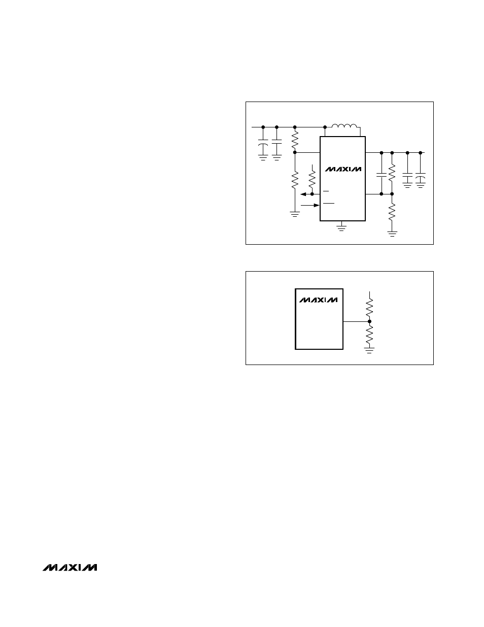
MAX1642
GND
BATT
PFI
V
OUT
= 2V
TO 5.2V
0.88V to 1.65V INPUT
*OPTIONAL COMPENSATION
100
µ
H
PF0
100pF*
SHDN
LX
OUT
FB
R1
R2
OUT
22
µ
F
0.1
µ
F
MAX1642
MAX1643
PFI
R3
V
TH
R4
Figure 4. Adjustable-Output Circuit
Figure 5. Power-Fail Detection Circuit