Detailed description, Pin description – Rainbow Electronics MAX1817 User Manual
Page 7
________________Detailed Description
The MAX1817 dual step-up converter is designed to
supply the main power and LCD bias for low-power,
hand-held devices. The MAX1817’s main step-up con-
verter includes a 0.35
Ω N-channel power MOSFET
switch and provides a fixed 3.3V or adjustable 2.5V to
5.5V output at up to 125mA from an input as low as
1.5V. The MAX1817’s LCD bias step-up converter
includes a high-voltage 1.1
Ω power MOSFET switch to
support as much as 5mA at 28V (Figure 1). During
startup, the MAX1817 extends the LCD MOSFET switch
minimum off-time, limiting surge current. Both convert-
ers require an inductor and external rectifier.
The MAX1817 runs in bootstrap mode, powering the IC
from the main step-up converter’s output. Independent
logic-controlled shutdown for the main and LCD step-
up converters reduces quiescent current to 0.1µA.
Main Step-Up Converter
The MAX1817 main step-up converter runs from a
+1.5V to +5.5V input voltage and produces a fixed 3.3V
or adjustable 2.5V to 5.5V output voltage as well as
biasing the internal control circuitry. The MAX1817
switches only as often as is required to supply sufficient
power to the load. This allows the converter to operate
at lower frequencies at light loads, improving efficiency.
The control scheme maintains regulation when the error
amplifier senses the output voltage is below the feed-
back threshold, turning on the internal N-channel MOS-
FET and initiating an on-time. The on-time is terminated
when the 0.75A current limit is reached or when the
maximum on-time is reached. The N-channel MOSFET
remains off until the inductor current drops to 0, forcing
discontinuous inductor current. At the end of a cycle,
the error comparator waits for the voltage at FB to drop
below the regulation threshold, at which time another
cycle is initiated.
The main step-up converter uses a startup oscillator to
allow it to start from an input voltage as low as +1.2V.
This is necessary since the control circuitry is powered
from the step-up converter output (OUT). When the
voltage at OUT is below the OUT undervoltage lockout,
a fixed 50% duty cycle drives the internal N-channel
MOSFET, forcing the main output voltage to rise. Once
MAX1817
Compact, High-Efficiency, Dual-Output
Step-Up DC-DC Converter
_______________________________________________________________________________________
7
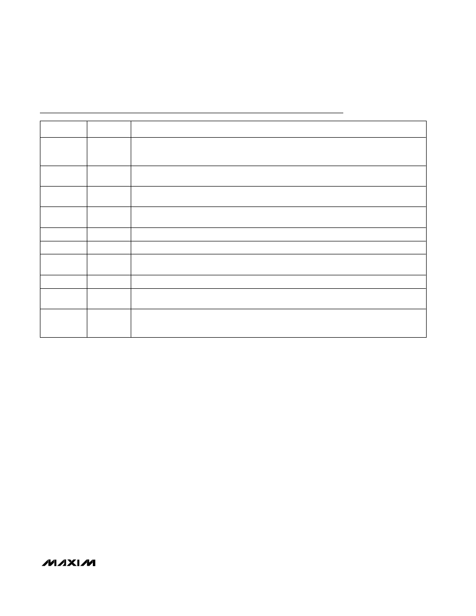
Pin Description
PIN
NAME
FUNCTION
1
FB
Main Output Feedback Input. Connect FB to GND for fixed 3.3V main output. For other output
voltages, use a resistive voltage-divider to set the output voltage. The feedback regulation voltage
is 1.25V at FB.
2
ON
Main Step-Up Converter On/Off Control. Connect ON to OUT for automatic startup. Connect ON to
GND to put the IC into shutdown mode.
3
ONLCD
LCD Output On/Off Control. Connect ONLCD to OUT to enable the LCD output. Connect ONLCD
to GND to disable the LCD output. The main output must be
≥2.4V to enable the LCD output.
4
FBLCD
LCD Output Feedback Input. Use a resistive voltage-divider from the LCD output to FBLCD to set
the voltage. The feedback regulation voltage is 1.25V at FBLCD.
5
AGND
Analog Ground. Connect AGND to GND as close to the IC as possible.
6
N.C.
No Connection. Not internally connected.
7
LXLCD
LCD Output Switching Node. Drain of the internal N-channel MOSFET that drives the LCD output.
Connect an external inductor and rectifier to LXLCD.
8
GND
Power Ground. Connect GND to AGND as close to the IC as possible.
9
LX
Main Output Switching Node. Drain of the internal N-channel MOSFET that drives the main output.
Connect an external inductor and rectifier to LX.
10
OUT
Main Step-Up Converter Output. OUT is used to measure the output voltage in fixed mode (FB =
GND) and is the internal bias supply input to the IC. When shut down (ON = ONLCD = GND), OUT
is high impedance, drawing 1µA (max).