Rainbow Electronics MAX1817 User Manual
Page 2
MAX1817
Compact, High-Efficiency, Dual-Output
Step-Up DC-DC Converter
2
_______________________________________________________________________________________
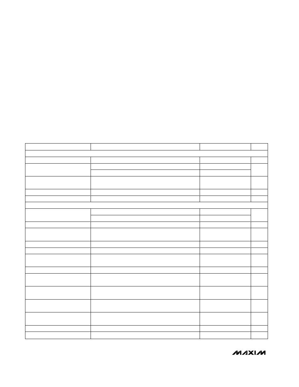
ABSOLUTE MAXIMUM RATINGS
ELECTRICAL CHARACTERISTICS
(V
ON
= V
ONLCD
= V
OUT
= +3.3V, FB = GND, T
A
= 0°C to +85°C, unless otherwise noted. Typical values are at T
A
= +25°C.)
Stresses beyond those listed under “Absolute Maximum Ratings” may cause permanent damage to the device. These are stress ratings only, and functional
operation of the device at these or any other conditions beyond those indicated in the operational sections of the specifications is not implied. Exposure to
absolute maximum rating conditions for extended periods may affect device reliability.
OUT to GND .............................................................-0.3V to +6V
ON, ONLCD, FB, FBLCD, LX to GND ......-0.3V to (V
OUT
+ 0.3V)
LXLCD to GND .......................................................-0.3V to +30V
AGND to GND .......................................................-0.3V to +0.3V
Continuous Power Dissipation (T
A
= +70°C)
10-Pin µMAX (derate 5.6mW/°C above +70°C) ...........444mW
LXLCD, LX Maximum Current ........................................0.5A
RMS
Operating Temperature Range ...........................-40°C to +85°C
Junction Temperature ......................................................+150°C
Storage Temperature Range .............................-65°C to +150°C
Lead Temperature (soldering, 10s) .................................+300°C
PARAMETER
CONDITIONS
MIN
TYP
MAX
UNITS
GENERAL
Input Voltage Range
1.5
5.5
V
R
LOAD
= 35
Ω
1.5
Startup Voltage
R
LOAD
=
∞,
V
FB
= 1.35V
1.2
1.55
V
Quiescent Current from OUT
(Main Only)
V
FB
= V
FBLCD
= 1.35V,
V
ONLCD
= 0
5
10
µA
Quiescent Current from OUT
V
FB
= V
FBLCD
= 1.35V
15
30
µA
Shutdown Quiescent Current
V
ON
= V
ONLCD
= 0
0.1
1
µA
MAIN OUTPUT
V
OUT
rising, V
FB
= 1.35V
2.2
2.4
OUT Undervoltage Lockout
V
OUT
falling, V
FB
= 1.35V
1.95
2.15
V
Fixed-Mode Output Voltage
V
FB
≤ 45mV
3.14
3.3
3.47
V
Adjustable-Mode FB Regulation
Voltage
1.20
1.25
1.30
V
FB Input Bias Current
V
FB
= 1.35V
50
nA
FB Dual Mode
TM
Threshold
45
75
105
mV
Output Voltage Adjustment
Range
2.5
5.5
V
Maximum LX On-Time
V
FB
= 0.5V
2.4
5
7.5
µs
Zero Crossing Comparator
Threshold (V
LX
- V
OUT
)
0
20
40
mV
Zero Crossing Comparator
Backup Timer
V
FB
= +0.5V
22
45
70
µs
Line Regulation
I
OUT
= 100mA,
V
IN
= +2V to +3V
1.6
%
Load Regulation
V
IN
= +2.5V,
I
LOAD
= 10mA to 100mA
1.6
%
LX On-Resistance
V
OUT
= 3.3V, I
LX
= 100mA
0.35
0.65
Ω
LX Current Limit
0.5
0.75
1.05
A
Dual Mode is a trademark of Maxim Integrated Products.