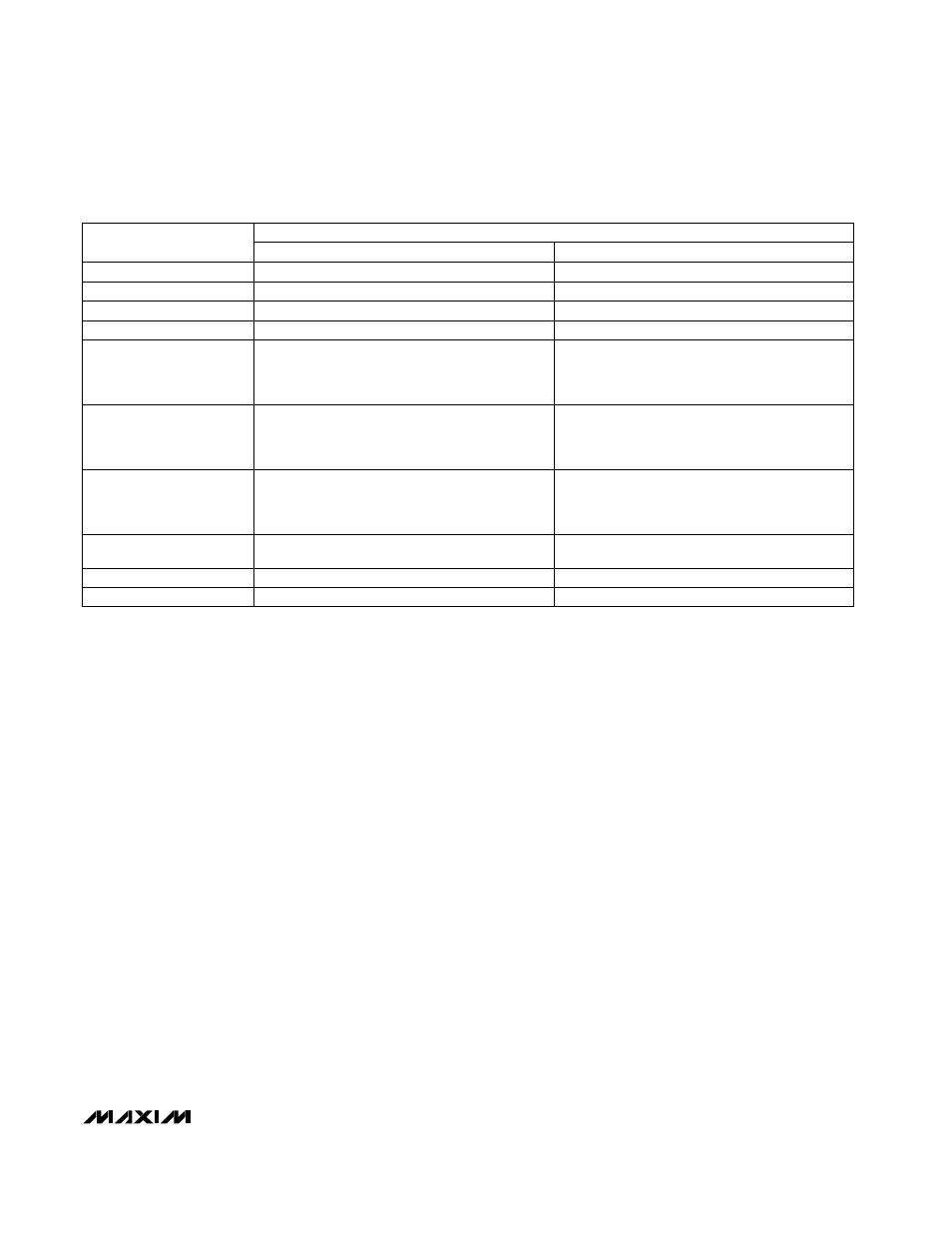
Table 1. component list for standard applications – Rainbow Electronics MAX1639 User Manual
Page 7
MAX1639
High-Speed Step-Down Controller with
Synchronous Rectification for CPU Power
_______________________________________________________________________________________
7
Table 1. Component List for Standard Applications
(x5) 560µF, Sanyo OS-CON 4SP560M
Central Semiconductor CMPSH-3
0.3µH, 25A, 0.9m
Ω
Panasonic ETQPAF0R3E
(x2) 7m
Ω
, Dale WSL-2512-R007-J
(x3) 330µF, Sanyo OS-CON 6SA330M
LOAD REQUIREMENT
Schottky diode, Motorola MBRD640
(x2) 0.010
Ω
, 30V, D
2
PAK, Fairchild FDB7030L
(x2) 0.014
Ω
, 30V, SO8, Fairchild FDS6680
(x2) 0.010
Ω
, 30V, D
2
PAK, Fairchild FDB7030L
(x2) 0.014
Ω
, 30V, SO8, Fairchild FDS6680
1.8V, 20A
C2
(x2) 560µF, Sanyo OS-CON 4SP560M
Central Semiconductor CMPSH-3
1.0µH, 9.3A, SMD
Coiltronics UP2B-1R0
1.0µH, 10A, SMD
Coilcraft D03316P-102HC
9m
Ω
Dale,
WSL-2512-R009-J
330µF, Sanyo OS-CON 6SA330M
D1 (optional)
Schottky diode, Nihon NSQ03A02
0.014
Ω
, 30V, SO8
Fairchild FDS6680
0.018
Ω
, 30V, SO8
International Rectifier IRF7413
N1
0.014
Ω
, 30V, SO8
Fairchild FDS6680
0.018
Ω
, 30V, SO8
International Rectifier IRF7413
D2
N2
2.5V, 8A
L1
R1
COMPONENT
C1
Note:
Parts used in evaluation board are shown in bold.
PWM Controller Block and Integrator
The heart of the current-mode PWM controller is a
multi-input, open-loop comparator that sums three sig-
nals (Figure 2): the buffered feedback signal, the cur-
rent-sense signal, and the slope-compensation ramp.
This direct-summing configuration approaches ideal
cycle-by-cycle control over the output voltage. The out-
put voltage error signal is generated by an error ampli-
fier that compares the amplified feedback voltage to an
internal reference.
Each pulse from the oscillator sets the main PWM latch
that turns on the high-side switch for a period deter-
mined by the duty factor (approximately V
OUT
/ V
IN
). The
current-mode feedback system regulates the peak
inductor current as a function of the output voltage error
signal. Since average inductor current is nearly the same
as peak current (assuming the inductor value is set rela-
tively high to minimize ripple current), the circuit acts as
a switch-mode transconductance amplifier. It pushes the
second output LC filter pole, normally found in a duty-
factor-controlled (voltage-mode) PWM, to a higher fre-
quency. To preserve inner-loop stability and eliminate
regenerative inductor current staircasing, a slope-
compensation ramp is summed into the main PWM com-
parator. Under fault conditions where the inductor cur-
rent exceeds the maximum current-limit threshold, the
high-side latch resets, and the high-side switch turns off.
Internal Reference
The internal 3.5V reference (REF) is accurate to ±1%
from 0°C to +85°C, making REF useful as a system ref-
erence. Bypass REF to AGND with a 0.1µF (min)
ceramic capacitor. A larger value (such as 2.2µF) is
recommended for high-current applications. Load reg-
ulation is 10mV for loads up to 100µA. Reference
undervoltage lockout is between 2.7V and 3V. Short-
circuit current is less than 4mA.
Synchronous-Rectifier Driver
Synchronous rectification reduces conduction losses in
the rectifier by shunting the normal Schottky diode or
MOSFET body diode with a low-on-resistance MOSFET
switch. The synchronous rectifier also ensures proper
start-up by precharging the boost-charge pump used
for the high-side switch gate-drive circuit. Thus, if you
must omit the synchronous power MOSFET for cost or
other reasons, replace it with a small-signal MOSFET,
such as a 2N7002.
The DL drive waveform is simply the complement of the
DH high-side drive waveform (with typical controlled
dead time of 30ns to prevent cross-conduction or
shoot-through). The DL output’s on-resistance is 0.7
Ω
(typ) and 2
Ω
(max).
10.0k
Ω
, 1%
10.0k
Ω
, 1%
R7
6.19k
Ω
, 1%
12.7k
Ω
, 1%
R8