Pin description – Rainbow Electronics MAX1639 User Manual
Page 5
MAX1639
High-Speed Step-Down Controller with
Synchronous Rectification for CPU Power
_______________________________________________________________________________________
5
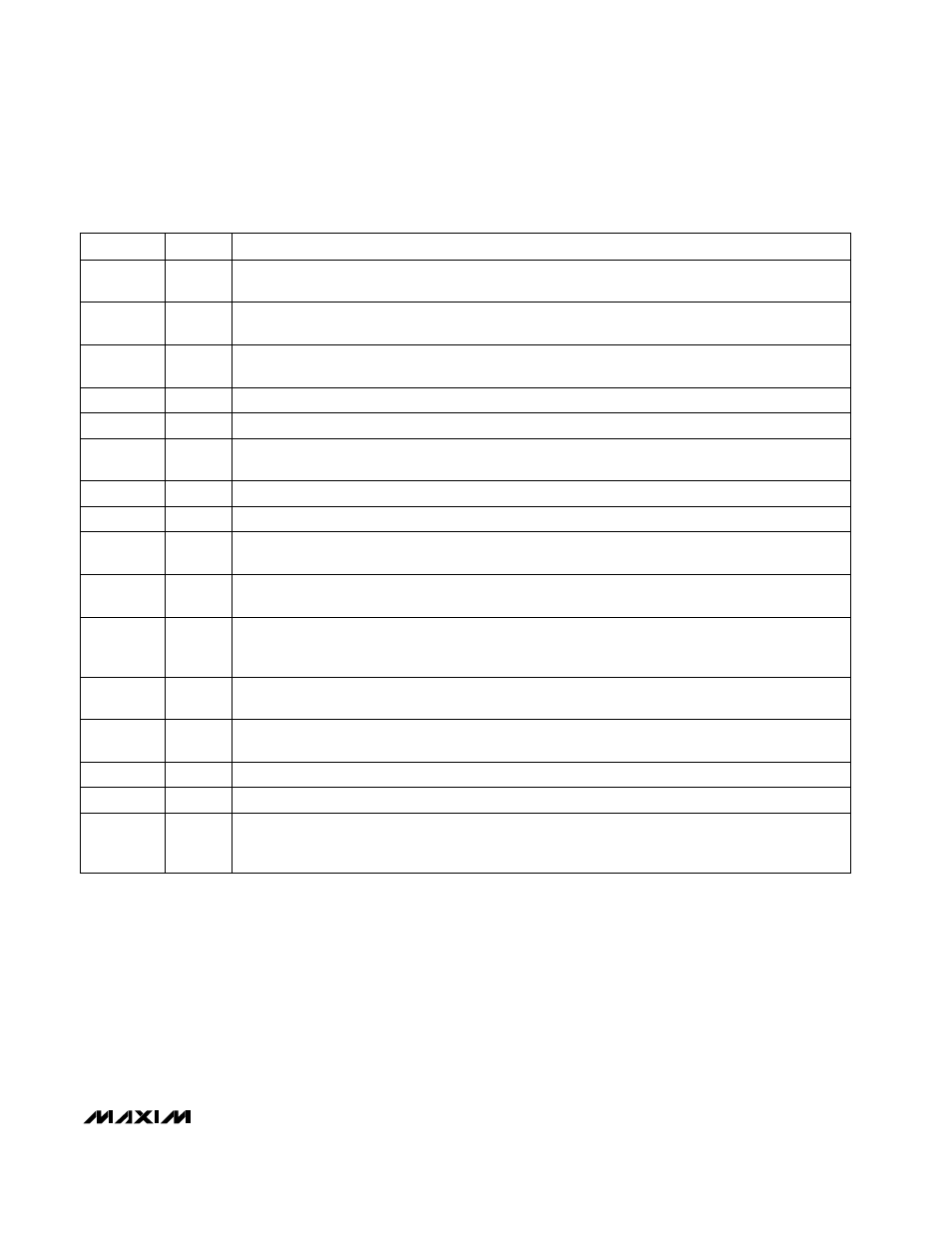
______________________________________________________________Pin Description
7
Analog Ground
AGND
6
Reference Output, 3.5V. Bypass REF to AGND with 0.1µF (min). Sources up to 100µA for external
loads. Force REF below 2V to turn off the controller.
REF
5
Analog Supply Input, 5V. Use an RC filter network, as shown in Figure 1.
V
CC
4
Current-Sense Amplifier’s Noninverting Input
CSH
3
Current-Sense Amplifier’s Inverting Input. Place the current-sense resistor very close to the controller IC,
and use a Kelvin connection.
CSL
2
Open-Drain Logic Output. PWROK is high when the voltage on FB is within +8% and -6% of its set-
point.
PWROK
8
Voltage-Feedback Input. The voltage at this input is regulated to 1.100V.
FB
9
Fast-Loop Compensation Capacitor Input. Connect a ceramic capacitor and resistor in series from
CC1 to AGND. See the section
Compensating the Feedback Loop
.
CC1
FUNCTION
NAME
1
Boost-Capacitor Bypass for High-Side MOSFET Gate Drive. Connect a 0.1µF capacitor and low-leak-
age Schottky diode as a bootstrapped charge-pump circuit to derive a 5V gate drive from V
DD
for DH.
BST
10
Slow-Loop Compensation Capacitor Input. Connect a ceramic capacitor from CC2 to AGND. See the
section
Compensating the Feedback Loop.
CC2
11
Frequency-Select Input. FREQ = V
CC
: 1MHz
FREQ = REF: 600kHz
FREQ = AGND: 300kHz
FREQ
12
Power Input for MOSFET Drivers, 5V. Bypass V
DD
to PGND within 0.2 in. (5mm) of the V
DD
pin using a
0.1µF capacitor and 4.7µF capacitor connected in parallel.
V
DD
13
Low-Side Synchronous Rectifier Gate-Drive Output. DL swings between PGND and V
DD
. See the
section
BST High-Side Gate-Driver Supply and MOSFET Drivers
.
DL
14
PGND
Power Ground
15
LX
Switching Node. Connect LX to the high-side MOSFET source and inductor.
16
DH
High-Side Main MOSFET Switch Gate-Drive Output. DH is a floating driver output that swings from LX
to BST, riding on the LX switching-node voltage. See the section
BST High-Side Gate-Driver Supply
and MOSFET Drivers
.
PIN