Applications information – Rainbow Electronics MAX1639 User Manual
Page 13
MAX1639
High-Speed Step-Down Controller with
Synchronous Rectification for CPU Power
______________________________________________________________________________________
13
large power diodes, such as the 1N4001 or 1N5817.
Exercise caution in the selection of Schottky diodes,
since some types exhibit high reverse leakage at high
operating temperatures. Bypass BST to LX using a
0.1µF capacitor.
Selecting the Input Capacitors
Place a 0.1µF ceramic capacitor and 10µF capacitor
between V
CC
and AGND, as well as between V
DD
and
PGND, within 0.2 in. (5mm) of the V
CC
and V
DD
pins.
Select low-ESR input filter capacitors with a ripple-
current rating exceeding the RMS input ripple current,
connecting several capacitors in parallel if necessary.
RMS input ripple current is determined by the input
voltage and load current, with the worst-possible case
occurring at V
IN
= 2 x V
OUT
:
__________Applications Information
Efficiency Considerations
Refer to the MAX796–MAX799 data sheet for informa-
tion on calculating losses and improving efficiency.
PC Board Layout Considerations
Good PC board layout and routing are
required
in high-
current, high-frequency switching power supplies to
achieve good regulation, high efficiency, and stability.
The PC board layout artist must be provided with explicit
instructions concerning the placement of power-switch-
ing components and high-current routing. It is strongly
recommended that the evaluation kit PC board layouts
be followed as closely as possible. Contact Maxim’s
Applications Department concerning the availability of
PC board examples for higher-current circuits.
In most applications, the circuit is on a multilayer
board, and full use of the four or more copper layers is
recommended. Use the top layer for high-current
power and ground connections. Leave the extra cop-
per on the board as a pseudo-ground plane. Use the
bottom layer for quiet connections (REF, FB, AGND),
and the inner layers for an uninterrupted ground plane.
A ground plane and pseudo-ground plane are essential
for reducing ground bounce and switching noise.
Place the high-power components (C1, R1, N1, D1, N2,
L1, and C2 in Figure 1) as close together as possible.
Minimize ground-trace lengths in high-current paths.
The surface-mount power components should be
butted up to one another with their ground terminals
almost touching. Connect their ground terminals using
a wide, filled zone of top-layer copper (the pseudo-
ground plane), rather than through the internal ground
plane. At the output terminal, use vias to connect the
top-layer pseudo-ground plane to the normal inner-
layer ground plane at the output filter capacitor ground
terminals. This minimizes interference from IR drops
and ground noise, and ensures that the IC’s AGND is
sensing at the supply’s output terminals.
Minimize high-current path trace lengths. Use very
short and wide traces. From C1 to N1: 0.4 in. (10mm)
max length; D1 anode to N2: 0.2 in. (5mm) max length;
LX node (N1 source, N2 drain, D1 cathode, inductor
L1): 0.6 in. (15mm) max length.
I
I
V
V
V
V
I
I
when V
V
RMS
LOAD MAX
OUT
IN
OUT
IN
RMS
OUT
IN
OUT
(
)
/
(
)
=
−
=
=
2
2
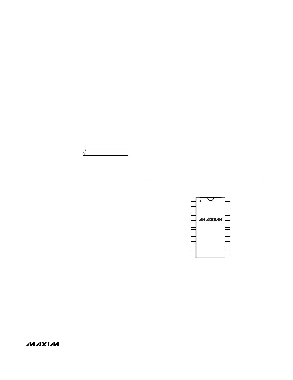
___________________Pin Configuration
___________________Chip Information
16
15
14
13
12
11
10
9
1
2
3
4
5
6
7
8
BST
DH
LX
PGND
DL
V
DD
FREQ
CC2
CC1
TOP VIEW
MAX1639
16 SOIC
PWROK
CSL
REF
CSH
V
CC
AGND
FB
TRANSISTOR COUNT: 3135
SUBSTRATE CONNECTED TO AGND