Table 1. configuration-byte format, Table 2. conversion-byte format – Rainbow Electronics MAX1099 User Manual
Page 15
MAX1098/MAX1099
10-Bit Serial-Output Temperature Sensors
with 5-Channel ADC
_______________________________________________________________________________________
15
Reference Selection
Select between internal and external voltage modes
through bit REF of the configuration byte. Set REF = 1
for internal reference mode and REF = 0 for external
reference mode.
Internal Reference
The MAX1098 has a 2.50V internal reference, while the
MAX1099 has a 1.20V internal reference. Both are fac-
tory trimmed for accuracy. When internal reference is
selected, REF can be used to drive an external load
with 100µA capability. Bypass REF to GND with a 0.1µF
minimum capacitance. Wake-up time is C x 2.5 x 10
4
s
for the MAX1098 and C x 1.2 x 10
4
s for the MAX1099.
External Reference
The MAX1098 can directly accept reference voltages at
REF from 0.8V to 2.5V, while the MAX1099 can directly
accept reference voltages from 0.8V to 1.2V. Bypass
REF to GND with a 0.1µF capacitor. Temperature mea-
surements always use internal reference.
Power Modes
The MAX1098/(MAX1099) typically requires supply cur-
rents of 380µA (350µA) or 310µA (280µA) when per-
forming voltage conversions at 100% duty cycle with
internal or external references, respectively. The differ-
Table 1. Configuration-Byte Format
BIT 7
(MSB)
BIT 6
BIT 5
BIT 4
BIT 3
BIT 2
BIT 1
BIT 0
(LSB)
Start
0
0
0
0
PM1
PM0
REF
BIT
NAME
DESCRIPTION
7 (MSB)
Start
First logic 1 after CS goes low. (See Input Data Format.)
6, 5, 4, 3
Must be 0000 to load a configuration byte.
2, 1
PM1, PM0
These 2 bits select the desired power mode (Table 3).
0
REF
A logic high enables the internal reference. A logic low disables the internal reference and
selects the external reference mode.
Table 2. Conversion-Byte Format
BIT 7
(MSB)
BIT 6
BIT 5
BIT 4
BIT 3
BIT 2
BIT 1
BIT 0
(LSB)
Start
0
1
0
SEL3
SEL2
SEL1
SEL0
BIT
NAME
DESCRIPTION
7 (MSB)
Start
First logic 1 after CS goes low. (See Input Data Format.)
6, 5, 4
Must be 010 to load a conversion byte.
3, 2, 1, 0
SEL3, SEL2,
SEL1, SEL0
These 4 bits select the input configuration (Table 4).
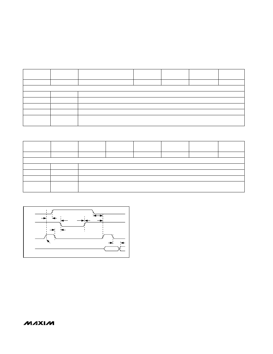
Figure 6. Detailed SSTRB Timing
t
CSH
t
DO
t
SSTRB
t
CONV
t
SCK
t
CSS
CSB
SSTRB
SCLK
DOUT
PDO CLOCKED IN
SSTRB TIMING