Absolute maximum ratings, Electrical characteristics – Rainbow Electronics MAX1791 User Manual
Page 2
MAX1762/MAX1791
High-Efficiency, 10-Pin µMAX, Step-Down
Controllers for Notebooks
2
_______________________________________________________________________________________
ABSOLUTE MAXIMUM RATINGS
VP, SHDN to GND ..................................................-0.3V to +22V
VP to VL ..................................................................-0.3V to +22V
OUT, VL to GND .......................................................-0.3V to +6V
DL, FB, REF to GND ....................................-0.3V to (VL + 0.3V)
DH to GND....................................................-0.3V to (VP + 0.3V)
CS to GND ....................................................-2.0V to (VP + 0.3V)
REF Short Circuit to GND ...........................................Continuous
Continuous Power Dissipation (T
A
= +70°C)
10-Pin µMAX (derate 5.6mW/°C above +70°C) ...........444mW
Operating Temperature .......................................-40°C to +85°C
Junction Temperature ......................................................+150°C
Storage Temperature.........................................-65°C to +150°C
Lead Temperature (soldering, 10s) .................................+300°C
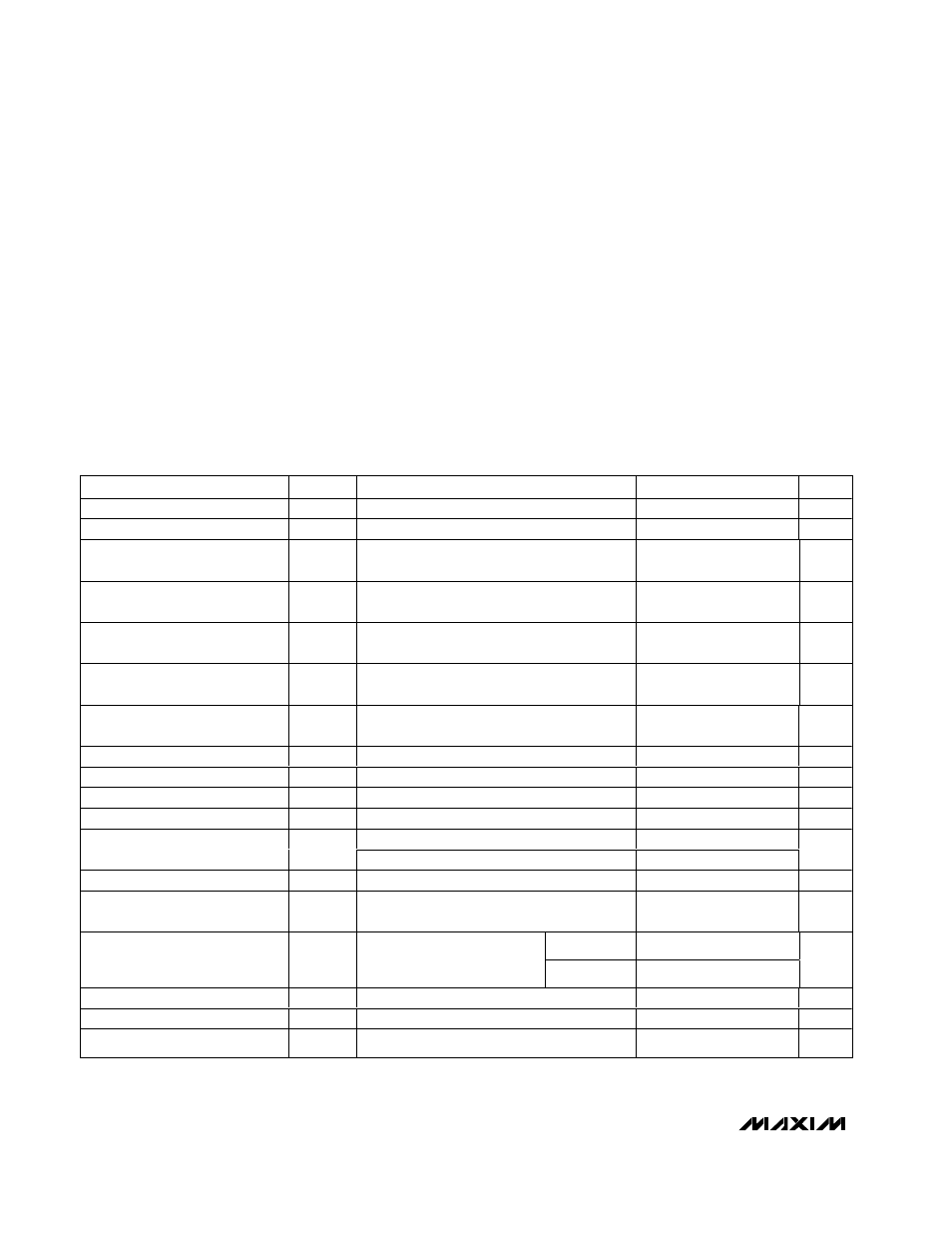
ELECTRICAL CHARACTERISTICS
(V
VP
= 15V, VL enabled, C
VL
= 1µF, C
REF
= 0.1µF, T
A
= 0 to +85°C, unless otherwise noted. Typical values are at T
A
= +25
°C.)
(Note 1)
PARAMETER
SYMBOL
CONDITIONS
MIN
TYP
MAX
UNITS
VP Input Voltage Range
V
VP
5
20
V
VL Input Voltage Range
V
VL
VL (overdriven)
4.75
5.25
V
OUT Output Voltage
(MAX1762, 1.8V Fixed)
V
OUT
V
VP
= 5V to 20V, V
VL
= 4.75V to 5.25V,
FB = GND, continuous conduction mode
1.773
1.8
1.827
V
OUT Output Voltage
(MAX1762, 2.5V Fixed)
V
OUT
V
VP
= 5V to 20V, V
VL
= 4.75V to 5.25V,
FB = VL, continuous conduction mode
2.463
2.5
2.538
V
OUT Output Voltage
(MAX1791, 3.3V Fixed)
V
OUT
V
VP
= 5V to 20V, V
VL
= 4.75V to 5.25V,
FB = GND, continuous conduction mode
3.250
3.3
3.350
V
OUT Output Voltage
(MAX1791, 5V Fixed)
V
OUT
V
VP
= 7V to 20V, V
VL
= 4.75V to 5.25V,
FB = VL, continuous conduction mode
4.925
5
5.075
V
OUT Output Voltage (Adj Mode)
V
VP
= 5V to 20V, V
VL
= 4.75V to 5.25V,
FB = OUT, continuous conduction mode
1.231
1.250
1.269
V
Output Voltage Adjust Range
0.5
5.5
V
OUT Input Resistance
Adjustable-output mode
300
800
1700
k
Ω
FB Input Bias Current
V
FB
= 1.3V
-0.1
0.1
µA
Soft-Start Ramp Time
Zero to full I
LIM
1700
µs
V
OUT
= 1.25V, V
VP
= 6V
666
740
814
On-Time (Note 2)
t
ON
V
OUT
= 5V, V
VP
= 6V
2550
2830
3110
ns
Minimum Off-Time (Note 2)
t
OFF
300
400
500
ns
VL Quiescent Supply Current
FB = GND, V
VL
= 5V, OUT forced above the
regulation point
153
260
µA
V
VL
= float
227
410
VP Quiescent Supply Current
FB = GND, OUT forced
above the regulation point,
V
VP
= 20V
V
VL
= 5V
93
200
µA
VL Shutdown Supply Current
V
VL
= 5V,
SHDN = GND
2
15
µA
VP Shutdown Supply Current
S HD N = GN D , m easur ed at V P , V
V L
= 0 or 5V
4
12
µA
VL Output Voltage
I
LOAD
= 0 to 25mA, V
VP
= 5V to 20V
4.5
4.65
4.75
V
Stresses beyond those listed under “Absolute Maximum Ratings” may cause permanent damage to the device. These are stress ratings only, and functional
operation of the device at these or any other conditions beyond those indicated in the operational sections of the specifications is not implied. Exposure to
absolute maximum rating conditions for extended periods may affect device reliability.