Rainbow Electronics MAX1791 User Manual
Page 18
MAX1762/MAX1791
High-Efficiency, 10-Pin µMAX, Step-Down
Controllers for Notebooks
18
______________________________________________________________________________________
a fixed +1.8V (MAX1762) or 3.3V (MAX1791) output.
Connect FB to VL for a fixed 2.5V (MAX1762) or 5.0V
(MAX1791) output. Otherwise, connect FB to a resistive
voltage-divider for an adjustable output.
Setting the Output Voltage
Select V
OUT
> 1.25V for the MAX1762/MAX1791 by
connecting FB to a resistive voltage-divider between
V
OUT
and GND (Figure 2). Choose R2 to be about
10k
Ω, and solve for R1 using the equation:
where V
FB
= 1.25V. For a V
OUT
= 3.0V, R2 = 10k
Ω and
R1 = 14k
Ω.
For a desired V
OUT
< 1.25V, connect FB to a resistive
voltage-divider between REF and OUT (Figure 3).
Choose R1 to be about 50k
Ω, and solve for R2 using
the equation:
where V
FB
= 1.25V and V
REF
= 2.0V. For a V
OUT
=
1.0V, R1 = 50k
Ω and R2 = 16.5kΩ. Under these condi-
tions, a minimum load of V
REF
- V
FB
/ R1 >15µA is
required.
PC Board Layout Guidelines
Careful PC board layout is critical to achieve low
switching losses and clean, stable operation. This is
especially true when multiple converters are on the
same PC board where one circuit can affect the other.
The switching power stages require particular attention
(Figure 10). Refer to the MAX1791 EV kit manual for a
specific layout example.
If possible, mount all of the power components on the
top side of the board, with their ground terminals flush
against one another. Follow these guidelines for good
PC board layout:
•
Isolate the power components on the top side from
the sensitive analog components on the bottom
side with a ground shield. Use a separate GND
plane under OUT. Avoid the introduction of AC cur-
rents into the GND ground planes. Run the power
plane ground currents on the top side only, if possi-
ble.
•
Keep the high-current paths short, especially at the
ground terminals. This practice is essential for sta-
ble, jitter-free operation.
•
Keep the power traces and load connections short.
This practice is essential for high efficiency. Using
thick copper PC boards (2oz vs. 1oz) can enhance
full-load efficiency by 1% or more. Correctly routing
PC board traces is a difficult task that must be
approached in terms of fractions of centimeters,
where a single milliohm of excess trace resistance
causes a measurable efficiency penalty.
•
Inductor and GND connections to the synchronous
rectifiers for current limiting must be made using
Kelvin sensed connections to guarantee the cur-
rent-limit accuracy. With SO-8 MOSFETs, this is
best done by routing power to the MOSFETs from
outside using the top copper layer, while connect-
ing GND and CS inside (underneath) the µMAX
package.
•
When trade-offs in trace lengths must be made, it’s
preferable to allow the inductor charging path to be
made longer than the discharge path. For example,
it’s better to allow some extra distance between the
input capacitors and the high-side MOSFET than to
allow distance between the inductor and the low-
side MOSFET or between the inductor and the out-
put filter capacitor.
•
Ensure that the OUT connection to C
OUT
is short
and direct. However, in some cases it may be desir-
able to deliberately introduce some trace length
between the OUT connector node and the output
filter capacitor (see Stability Considerations).
•
Route high-speed switching nodes (CS, DH, and
DL) away from sensitive analog areas (FB). Use
GND as an EMI shield to keep radiated switching
noise away from the IC’s feedback divider and ana-
log bypass capacitors.
R2
V
- V
V
- V
R1
OUT
FB
FB
REF
=
×
V
V
R1
R2
OUT
FB
=
× +
1
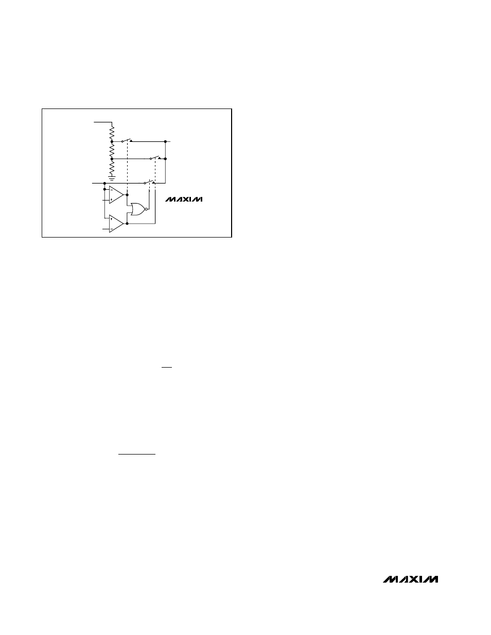
Figure 9. Feedback MUX
MAX1762
TO ERROR
AMP
0.150V
2.5V
FB
FIXED
1.8V
FIXED
3.3V
OUT