Chip topography, Table 2. component suppliers – Rainbow Electronics MAX1655 User Manual
Page 11
Input Bypass Capacitor
The input bypass capacitor reduces peak currents
drawn from the voltage source, and also reduces the
amount of noise at the voltage source caused by the
switching action of the MAX1649/MAX1651. The input
voltage source impedance determines the size of the
capacitor required at the V+ input. As with the output fil-
ter capacitor, a low-ESR capacitor is recommended.
Bypass the IC separately with a 0.1µF ceramic capac-
itor placed close to the V+ and GND pins.
Reference Capacitor
Bypass REF with a 0.1µF or larger capacitor.
MAX1649/MAX1651
5V/3.3V or Adjustable, High-Efficiency,
Low-Dropout, Step-Down DC-DC Controllers
______________________________________________________________________________________
11
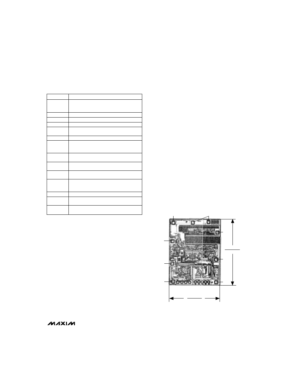
___________________Chip Topography
TRANSISTOR COUNT: 428
SUBSTRATE CONNECTED TO V+
0.106"
(2.692mm)
0.081"
(2.057mm)
OUT
GND
CS
EXT
V+
FB
SHDN
REF
Table 2. Component Suppliers
COMPANY
PHONE
FAX
(207) 282-5111
AVX
USA
or
(207) 283-1941
(800) 282-4975
Coiltronics
USA
(407) 241-7876
(407) 241-9339
CoilCraft
USA
(708) 639-6400
(708) 639-1469
Dale
USA
(402) 564-3131
(402) 563-1841
International
USA
(310) 322-3331
(310) 322-3332
Rectifier
IRC
USA
(512) 992-7900
(512) 992-3377
(602) 244-3576
Motorola
USA
or
(602) 244-4015
(602) 244-5303
Nichicon
USA
(708) 843-7500
(708) 843-2798
Japan
81-7-5231-8461
81-7-5256-4158
Nihon
USA
(805) 867-2555
(805) 867-2556
Japan
81-3-3494-7411
81-3-3494-7414
Sanyo
USA
(619) 661-6835
(619) 661-1055
Japan
81-7-2070-6306
81-7-2070-1174
(408) 988-8000
Siliconix
USA
or
(408) 970-3950
(800) 554-5565
Sprague
USA
(603) 224-1961
(603) 224-1430
Sumida
USA
(708) 956-0666
(708) 956-0702
Japan
81-3-3607-5111
81-3-3607-5144
United
USA
(714) 255-9500
(714) 255-9400
Chemi-Con
Layout Considerations
Proper PC board layout is essential because of high
current levels and fast switching waveforms that radi-
ate noise. Minimize ground noise by connecting the
anode of the rectifier, the input bypass capacitor
ground lead, and the output filter capacitor ground
lead to a single point (“star” ground configuration). A
ground plane is recommended. Also minimize lead
lengths to reduce stray capacitance, trace resistance,
and radiated noise. In particular, the traces connected
to FB (if an external resistor divider is used) and EXT
must be short. Place the 0.1µF ceramic bypass capac-
itor as close as possible to the V+ and GND pins.
MAX1649/MAX1651 vs. MAX649/MAX651
The MAX1649 and MAX1651 are pin compatible with
the MAX649 and MAX651, but have been optimized for
improved dropout performance and efficiency—partic-
ularly with low input voltages. The MAX1649/MAX1651
feature increased maximum switch duty cycle (96.5%)
and reduced current-limit sense voltage (110mV).
Their predecessors, the MAX649/MAX651, use a high-
er two-step (210mV/110mV) current-limit sense voltage
to provide tighter current-sense accuracy and reduced
inductor peak current at light loads.