Detailed description, Pin description – Rainbow Electronics MAX711 User Manual
Page 6
_______________Detailed Description
The MAX710/MAX711 integrate a step-up DC-DC con-
verter with a linear regulator to provide step-up/down
voltage conversion. The step-up switch-mode regulator
contains an N-channel power MOSFET switch. It also
shares a precision voltage reference with a linear regu-
lator that contains a P-channel MOSFET pass element
(Figure 1).
Step-Up Operation
A pulse-frequency-modulation (PFM) control scheme
with a constant 1µs off-time and variable on-time con-
trols the N-channel MOSFET switch. The N-channel
switch turns off when the part reaches the peak current
limit or the 4µs maximum on-time. The ripple frequency
is a function of load current and input voltage.
Step-Down Operation
The low-dropout linear regulator consists of a refer-
ence, an error amplifier, and a P-channel MOSFET. The
reference is connected to the error amplifier’s inverting
input. The error amplifier compares this reference with
the selected feedback voltage and amplifies the differ-
ence. The difference is conditioned and applied to the
P-channel pass transistor’s gate.
Operating Configurations
The MAX710/MAX711 have several operating configu-
rations to minimize noise and optimize efficiency for dif-
ferent input voltage ranges. These configurations are
accomplished via the N/E input, which controls opera-
tion of the on-chip linear regulator.
With N/E low, the linear regulator behaves as a 0.7
Ω
(at
5V output) PFET switch when the IC is boosting, and as
a conventional linear regulator when V
IN
> V
OUT
. This
provides optimum boost efficiency, but the PFET does
little to reject boost-converter output ripple. With N/E
high, boost ripple rejection is optimized by maintaining
headroom (V
FV
, typically 0.5V at 5V output) across the
linear regulator. Boost mode efficiency is then about
10% lower than with N/E high.
MAX710/MAX711
3.3V/5V or Adjustable,
Step-Up/Down DC-DC Converters
6
_______________________________________________________________________________________
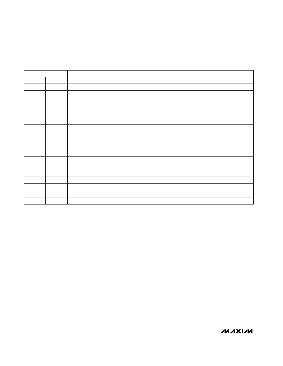
______________________________________________________________Pin Description
Drain Connection for internal N-channel power MOSFET
LX
1
Power Ground
PGND
2
Shutdown Input. When low, the entire circuit is off and OUT is actively pulled to GND.
SHDN
4
Inductor Current-Limit-Select Input. Connect to GND for 1.5A limit and to PS for 0.8A limit.
ILIM
3
Standby Input. Connect to GND to disable boost circuit. Connect to PS for normal operation.
STBY
5
Selects low-noise or high-efficiency mode. Connect to GND for high efficiency and to PS for
lowest noise. See
Operating Configurations
section.
N/E
7
Selects the output voltage. Connect to GND for 5V output and to OUT for 3.3V output.
3/5
6
2
4
3
5
7
—
1
Low-Battery Comparator Output
LBO
8
8
Negative Input to Low-Battery Comparator
LBI-
10
Source of internal PFET regulator. The IC is powered from PS.
PS
12
Positive Input to Low-Battery Comparator
LBI+
11
1.28V Reference Voltage Output. Bypass with a 0.1µF capacitor to GND.
REF
13
Power Ground
PGND
15
Analog Ground. Must be low impedance. Solder directly to ground plane.
GND
14
10
12
11
13
15
14
9
Drain Connection for internal N-channel power MOSFET
LX
16
16
Linear-Regulator Output. Bypass with a 4.7µF capacitor to GND.
OUT
9
MAX711
MAX710
FUNCTION
NAME
PIN
Feedback Input
FB
—
6